I tried to follow the below article from Infineon for gate resistance calculation GateResistance for method1 based on the switching time, my doubt is for the gate driver in case 2 Mosfets are connected instead of 1 Mosfet will gate resistance will increase or decrease and by what factor will it be kind of 2? Please help with calculations. It is too complicated for me to understand the parameters and calculations.
You are using an out of date browser. It may not display this or other websites correctly.
You should upgrade or use an alternative browser.
You should upgrade or use an alternative browser.
Scroll to continue with content
The input capacitance will be doubled, so will input driving current, hence the gate resistance needs to be halved to retain the same switching time.in case 2 Mosfets are connected instead of 1 Mosfet will gate resistance will increase or decrease and by what factor will it be kind of 2?
Thank you for reply, but one challenge i am facing is for the Mosfet driver attached i am unable to find the table similar to belowThe input capacitance will be doubled, so will input driving current, hence the gate resistance needs to be halved to retain the same switching time.

which is used in the calculation
Can you please guide how do i calculate for the driver i have attached. There is an article from Infineon but could not follow
InternalResistance
Thank you in advance.
Attachments

Ok, now i get it thank you,I think this section of Fig 5 has the information you need :-
View attachment 69835
Internal source resistance Calculation
Rs1 Ohm = VCC/IOpk+ = 15 Volts / 2.5 A = 6 Ohm
Rs2 Ohm = Voh / Itest = 0.05 Volts / 0.02 A = 2.5 Ohm
Average = (Rs1 + Rs2) / 2 = (6 Ohm + 2.5 Ohm)/2 = 4.25 Ohm
So, the internal source resistance is 4.25Ohm
Internal Sink Resistance Calculation
Rs1 Ohm = 15 Volts / 2.5 A = 6 Ohm
Rs2 Ohm = Vol volts / I test A = 0.02 Volts / 0.02 A = 1 Ohm
Average = (6 Ohm + 1 Ohm) / 2 = 3.5 Ohm
Sink resistance = 3.5 Ohm
Only one clarification, if i am operating the driver at 12V the calculations remain same or will it change?
Please help to review and confirm the calculations for the total gate resistance the Mosfet data sheet i have attached, the gate resistance calculations are performed as per the article GateResistance
tsw = 100ns, the way i arrived at 100ns is the switching frequency is 15KHz , time for one cycle = 1/15KHz = 66uSec
for 1% duty the time will 66uSec/100 = 666nSec
Step1:
As per the data sheet

Qgs = 35nC
Qgd = 43nC
Iavg A = (35nC + 43nC)/ 100 nS = 0.78 A
Step2:
Vcc is turn on gate voltage
Vge gate plateau voltage
Vcc = 12V given to the Mosfet driver
Vge = 5V as per the below diagram from data sheet

RTot Ohm = (12V - 5V)/0.78 A = 8.9 Ohm
RTot Ohm = Rgon Ohm + Rdrp Ohm
Rgon Ohm = RTot Ohm - Rdrp Ohm (Rdrp = 4.25 Ohm from previous post calculations)
= 8.9 Ohm - 4.25 Ohm
Rgon = 4.72 Ohm for 1 Mosfet
Since 2 Mosfets are connected the Rgon will be halved
Hence the Rgon = 2.36 Ohm
Request to please confirm if it is the correct value as per calculations. Thank you in advance for your time.
tsw = 100ns, the way i arrived at 100ns is the switching frequency is 15KHz , time for one cycle = 1/15KHz = 66uSec
for 1% duty the time will 66uSec/100 = 666nSec
Step1:
As per the data sheet
Qgs = 35nC
Qgd = 43nC
Iavg A = (35nC + 43nC)/ 100 nS = 0.78 A
Step2:
Vcc is turn on gate voltage
Vge gate plateau voltage
Vcc = 12V given to the Mosfet driver
Vge = 5V as per the below diagram from data sheet
RTot Ohm = (12V - 5V)/0.78 A = 8.9 Ohm
RTot Ohm = Rgon Ohm + Rdrp Ohm
Rgon Ohm = RTot Ohm - Rdrp Ohm (Rdrp = 4.25 Ohm from previous post calculations)
= 8.9 Ohm - 4.25 Ohm
Rgon = 4.72 Ohm for 1 Mosfet
Since 2 Mosfets are connected the Rgon will be halved
Hence the Rgon = 2.36 Ohm
Request to please confirm if it is the correct value as per calculations. Thank you in advance for your time.
Attachments
I am sorry i could not understand completely what you are trying to say, whatever little i can understand is that we cannot completely rely on the calculations, based on testing we have to decide the value, am i correct?The calculation gives you a non optimal value as trace Z, especially the L,
and device to device variations produce a non optimal value. But as always]
its a best effort compromise. In one off designs some folks trim them.
Martaine2005
- May 12, 2015
- 5,284
- Joined
- May 12, 2015
- Messages
- 5,284
Yes, that’s correct.I am sorry i could not understand completely what you are trying to say, whatever little i can understand is that we cannot completely rely on the calculations, based on testing we have to decide the value, am i correct?
The math may be correct but the real world characteristics and tolerances of components including circuit board traces all affect the final values.
So either a compromise or a slight change of component value can achieve the desired result.
We are always dealing with non-exact models, hence the calculations, for the non-exact model,
can meet all our rules on Thevenin's rules for analyzing circuits, but the model being inexact gives
us approximations. Much of the time we can use the approximations and move on, but there are
times in design where we use testing and characterization procedures to "finalize" the design. So
in your prior calculations you clearly notice nothing is present on PCB layout right ? But those traces,
their width, length, dielectric material, ground plane .....in some designs, especially RF type designs,
are used in modeling.
Now for this design you can generate ringing when working with MOSFETs in their gate circuit due
to a number of factors. So nominally you do the calc, fire up the design and examine the gate with
a fast scope to see if the gate node at device is ringing, if it is the R is too low a value to dampen the
Q, the L effects, in the drive path. But as we raise that R to do so, if needed, we start affecting rise
and fall times and hence power in the MOSFET, tradeoffs, always tradeoffs.
I am not trying to overwhelm you, just trying to fill in the edges of what one can experience when working
with MOSFETs and their non ideal behavior. Like Miller C effects as well.
As an aside good scope probing practices important :
https://www.testequity.com/UserFiles/documents/pdfs/tektronix/probe_fundamentals.pdf
Last edited:
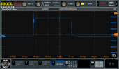
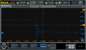
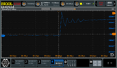
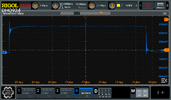
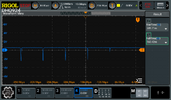
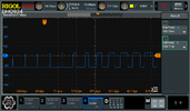
Yes exactly i am facing the ringing issue at Gate to Source Low side after the Mosfet driver, i have not verified at high side. At some levels of modulation index of 85% the ringing is very high and over voltage fault is created. That is the reason i went for the exact calculation of external gate resistance, as of now it is 22 Ohm (two 22 ohm for 2 Mosfets) and as per calculation it is coming around 2.36 so i will try with different values of resistances. Please suggest recommendations to rectify the issue. (Running FOC, SVPWM, BLDC motor, 10 poles)
Attachments
Show a pic of your probing/prototype/layout. Your probe ground lead real short...?
If thats the case simply raise the gate R.
Post schematic of driver and MOSFET wiring/layout.
That MOSFET super high C so challenging for sure.
That gate drive waveform, scope not set for 10X probe ? The waveform shows roughly
600 mV drive ? Is that really 6V ?
Bypass capacitors ESR very important, combo of cermaic and Tant (Polymer preferred) -

What does supply rail look like on scope, use infinite persistence, AC coupled, say 10 uS/box, verical 50 mV/box,
+edge trigger, say 50 mV....
If thats the case simply raise the gate R.
Post schematic of driver and MOSFET wiring/layout.
That MOSFET super high C so challenging for sure.
That gate drive waveform, scope not set for 10X probe ? The waveform shows roughly
600 mV drive ? Is that really 6V ?
Bypass capacitors ESR very important, combo of cermaic and Tant (Polymer preferred) -
What does supply rail look like on scope, use infinite persistence, AC coupled, say 10 uS/box, verical 50 mV/box,
+edge trigger, say 50 mV....
Last edited:
Sorry i did not explain the testingShow a pic of your probing/prototype/layout. Your probe ground lead real short...?
If thats the case simply raise the gate R.
Post schematic of driver and MOSFET wiring/layout.
That MOSFET super high C so challenging for sure.
That gate drive waveform, scope not set for 10X probe ? The waveform shows roughly
600 mV drive ? Is that really 6V ?
Bypass capacitors ESR very important, combo of cermaic and Tant (Polym
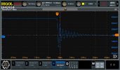
The probe is differential probe positive on the gate output, pin no 4

and negative on the battery ground instead of the source. The probe is in *20 mode hence 0.6V will be 0.6*20 = 12V. Pin 5 i gave 12V supply. Diffprobe
I will share the schematics shortly.
Last edited:
- Joined
- Nov 17, 2011
- Messages
- 14,280
This point does not account for the effect of the gate resistor. Put your probe directly to the gate of the MOSFET.probe is differential probe positive on the gate output, pin no 4
This introduces a long path for the current from the soure to your probe. Together with the accompanying inductance of the trace this can lead to ringing of the scope signal. Put your probe directly to teh source of the MOSFET.negative on the battery ground instead of the source.
Only with both probes directly at the MOSFET's pins and and the wire loop between the two probes as small as possible will you see the actual gate drive signal as the MOSFET experiences it.
Ok I will do it and share the waveforms.This point does not account for the effect of the gate resistor. Put your probe directly to the gate of the MOSFET.
This introduces a long path for the current from the soure to your probe. Together with the accompanying inductance of the trace this can lead to ringing of the scope signal. Put your probe directly to teh source of the MOSFET.
Only with both probes directly at the MOSFET's pins and and the wire loop between the two probes as small as possible will you see the actual gate drive signal as the MOSFET experiences it.
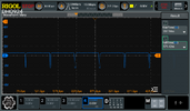
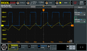
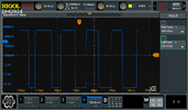
Yes i have taken the waveforms positive on the Mosfet Gate and negative on the source. One waveform i have taken with negative on battery ground. The number in the front indicates the modulation index. The waveforms are ok now. But 2 issues i have right now
a. when i set the modulation index to around 85% immediately it goes to overvoltage fault, i can see huge overcurrent fault in the battery kind of shoot through. If i update the software with 90% MI upto 93% it is ok, i can't go above 93% again over voltage fault. Anything upto 80% it is fine.
50% - 80% MI - No problem
83% - 90% MI - Motor does not run shoot through scenario
90 % - 93% MI - Motor running is ok (but need to run continuously)
b. The main reason i am trying to go to high MI is i have not yet acheived the motor max speed. At present i can go upto 2600 RPM but the motor capability is 3000 RPM, hence i want to change the Gate resistance to around 4 Ohms to reduce the rise and fall time. Please guide to address these issues. (I am running STM32 Motor control software).
Attachments

- Joined
- Nov 17, 2011
- Messages
- 14,280
Go ahead and give it a try. A bit of trial and error doesn't hurt, see post #9.i want to change the Gate resistance to around 4 Ohms
As a first step i reduced the gate resistance to 10 Ohm in place of 22 Ohm but no difference in speed is observed. I do not think further decrease in resistance will have impact on speed. I am not sure what else i can do to increase the speed, i am assuming FOC SVPWM gives the maximum speed, is there any other algorithm which can give improve the speed without flux weakening. It has to do with the algorithm or issue with the hardware? Any recommendations based on your experience, i have to increase minimum by another 200 RPM speed.
- Joined
- Nov 17, 2011
- Messages
- 14,280
What is the max. speed you achieve when you tie the gate of the MOSFET permanently high?
What speed does the motor reach when dirctly connected to the power supply without the intervening MOSFET?
What is gate voltage driving the on state? Note that the MOSFEt you use has a gate threshold voltage of 2 V - 4 V as per the datasheet you supplied. When you happen to have one of the more 4 V-ish specimens at hand, it may not be completely on. Many of the parameters in the datasheet are given for a gate-source voltage of 10 V or higher:

You may need a level shifter to drive the MOSFET with a gate voltage considerably higher than 5 V more like 10 V or 12 V.
Can you post the schematic for the relevant part of your circuit?
What speed does the motor reach when dirctly connected to the power supply without the intervening MOSFET?
What is gate voltage driving the on state? Note that the MOSFEt you use has a gate threshold voltage of 2 V - 4 V as per the datasheet you supplied. When you happen to have one of the more 4 V-ish specimens at hand, it may not be completely on. Many of the parameters in the datasheet are given for a gate-source voltage of 10 V or higher:
You may need a level shifter to drive the MOSFET with a gate voltage considerably higher than 5 V more like 10 V or 12 V.
Can you post the schematic for the relevant part of your circuit?
Delta Prime
- Jul 29, 2020
- 2,989
- Joined
- Jul 29, 2020
- Messages
- 2,989
Based on my experience, it sounds like a laboratory assignment given by your instructor. I use that term loosely.algorithm or issue with the hardware? Any recommendations based on your experience, i have to increase minimum by another 200 RPM speed
Be straightforward and tell us your application we’re here to help you and your instructor.
Similar threads
- Replies
- 2
- Views
- 10K
- Replies
- 23
- Views
- 619
- Replies
- 3
- Views
- 1K
- Replies
- 6
- Views
- 1K