Dual MOSFET Driver – Two Channel DC SSR Using MOSFETS & Gate Driver
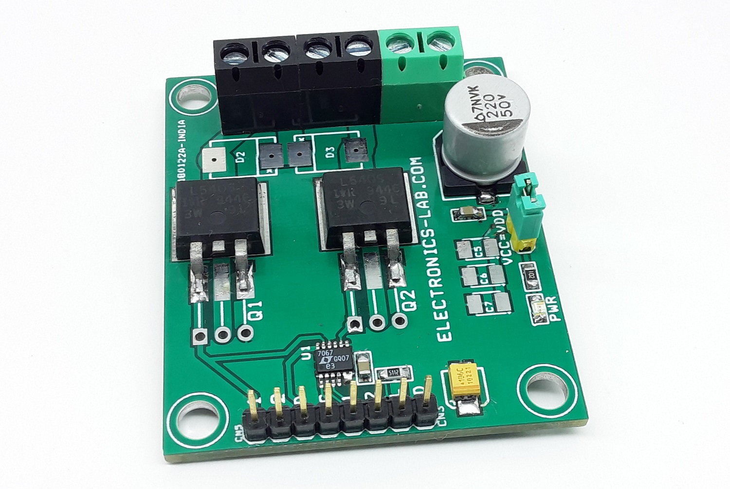
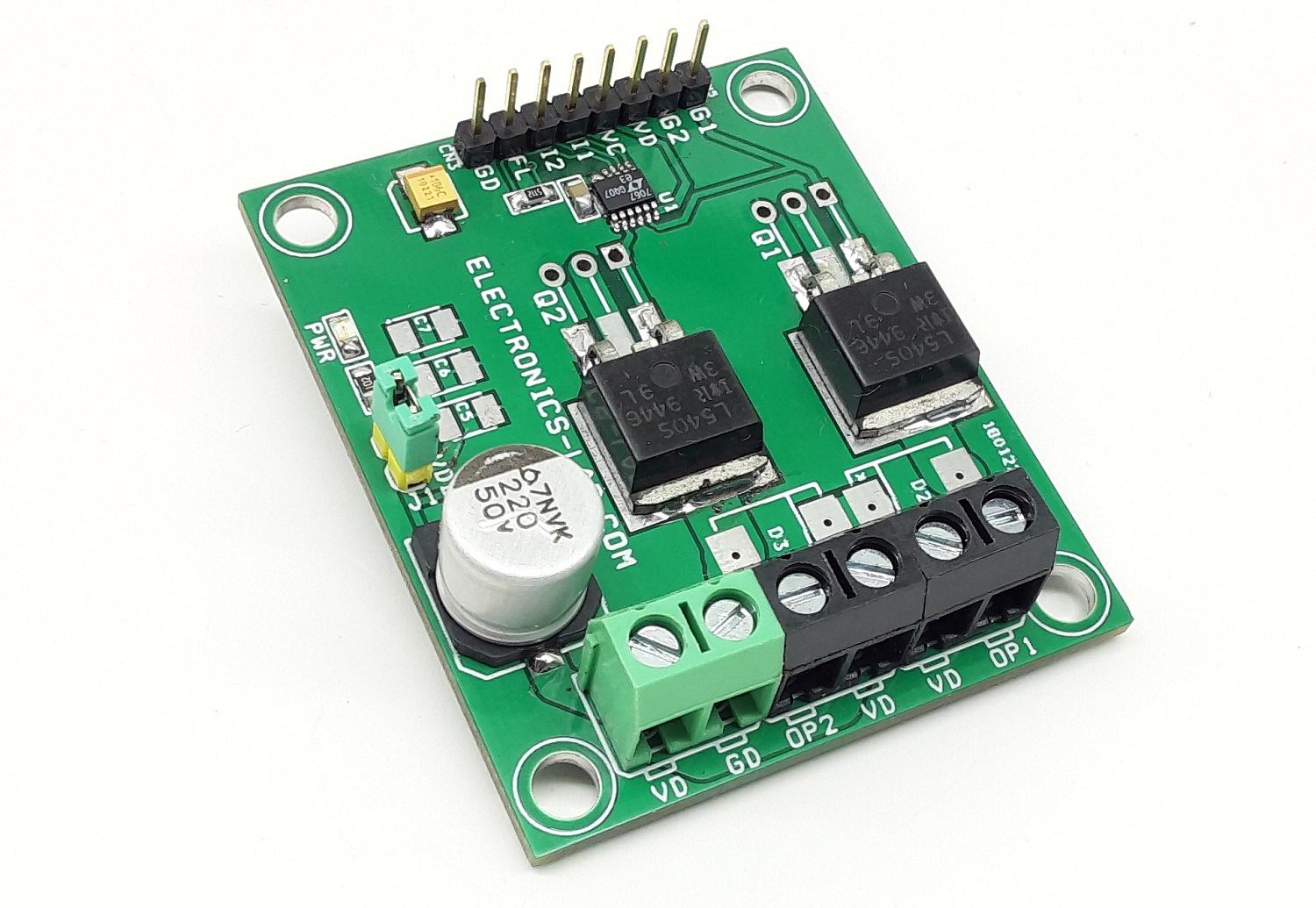
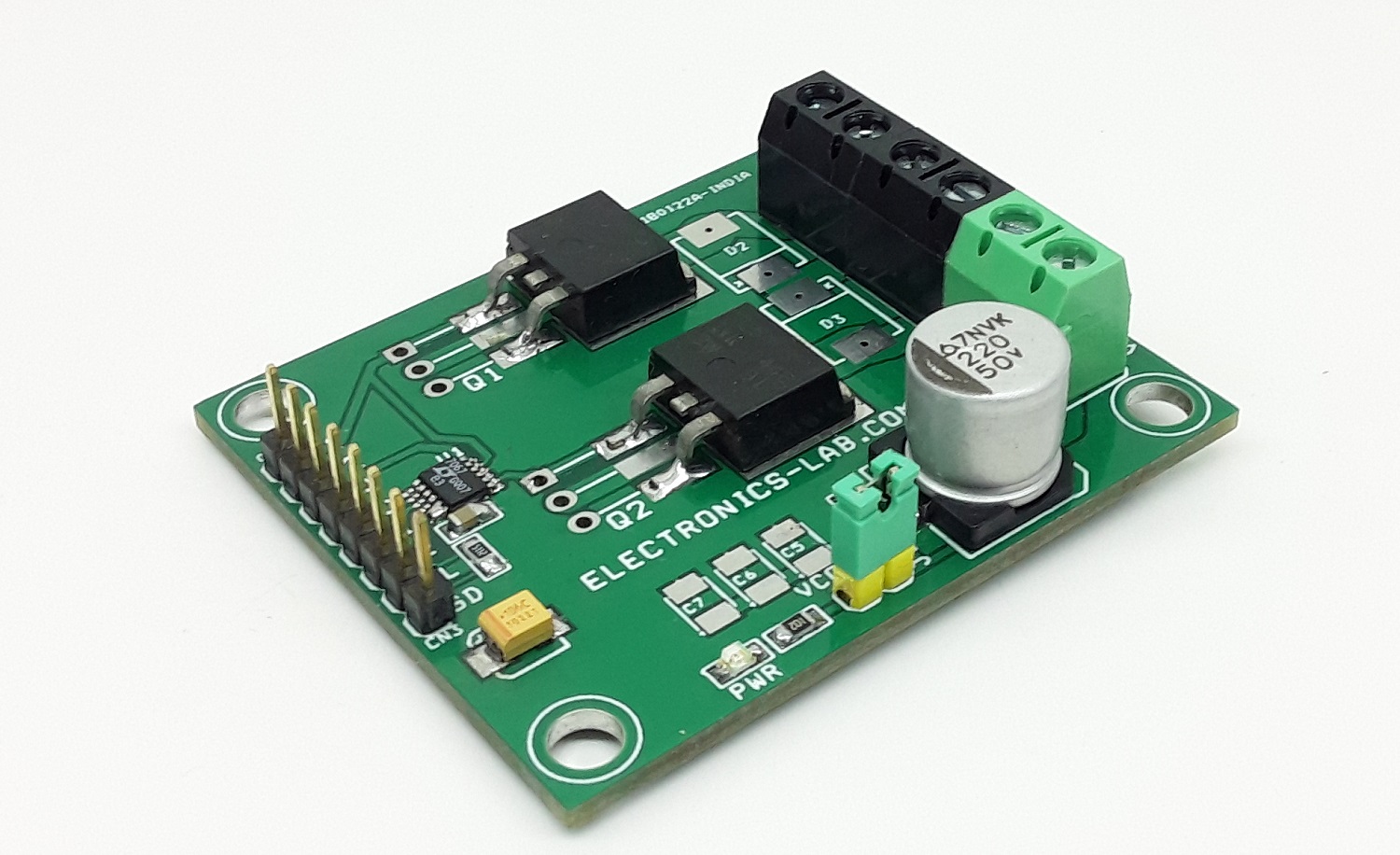
The project presented here is a dual-channel MOSFET DC relay. The project is capable of driving a 5A load on each channel with an input supply of 48V DC.
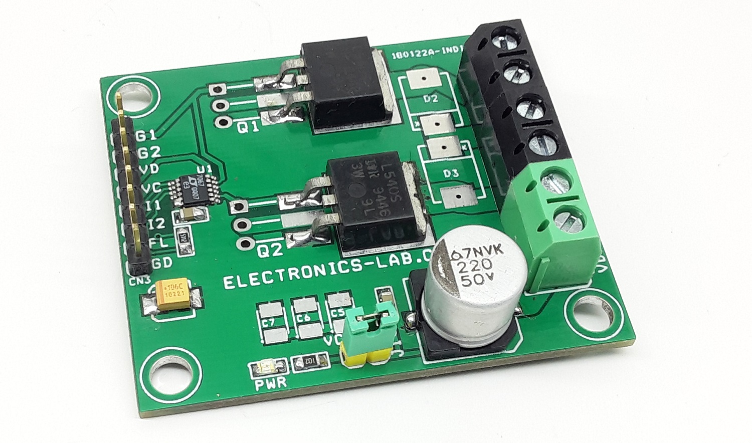
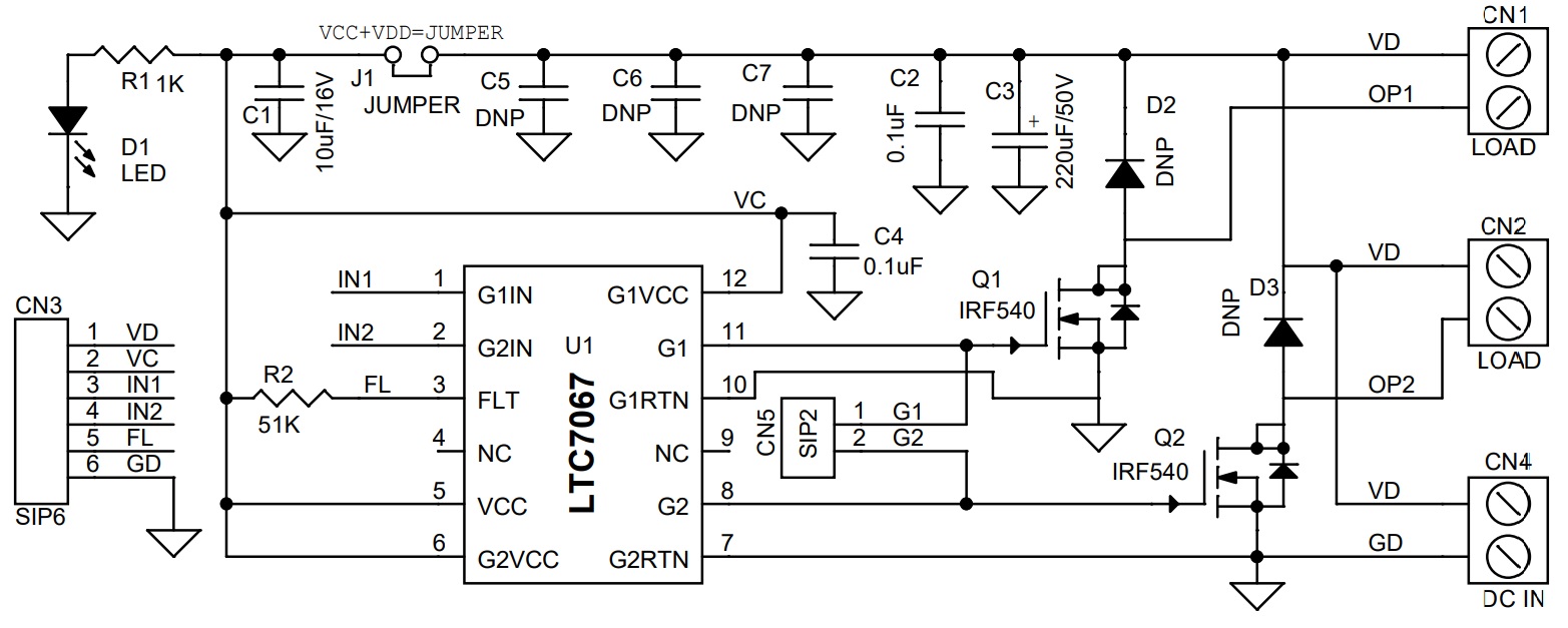
The project presented here is a dual-channel MOSFET DC relay. The project is capable of driving a 5A load on each channel with an input supply of 48V DC. The LTC7067 chip drives the two high-side N-Channel MOSFETS with supply voltages up to 48V DC. Its powerful 0.8Ω pull-down and 1.5Ω pull-up MOSFET drivers allow the use of large gate capacitance and high voltage MOSFETs. Additional features include UVLO, TTL/CMOS compatible inputs, and fault indicator. The optional diodes D2 and D3 can be used for inductive loads. Open-Drain Fault Output is available. The open-drain output pulls to GND during VCC UVLO/OVLO and floating supplies UVLO condition.
Features
- VDD (Load Supply) 12V to 48V DC
- VCC for Gate Driver 12-14V DC
- Load 5A Each Channel with Forced Air Cooling (Fan)
- On-Board Jumper for 12V-14V Single Supply Operations for Load and Gate Driver
- Fault Condition Output Normally High, Goes Low When UVLO/OVLO and Floating Supplies UVLO Condition Occurs
- Optional Clamp Diode D2, D3 for inductive Loads
- TTL/CMOS Compatible Control Inputs
- Input PWM Duty Cycle 0 to 100%
- Input Frequency 20Khz-Tested (Supports Higher Frequency)
- Under Voltage Lockout
- 4 x 3MM Mounting Holes
- Onboard Power LED
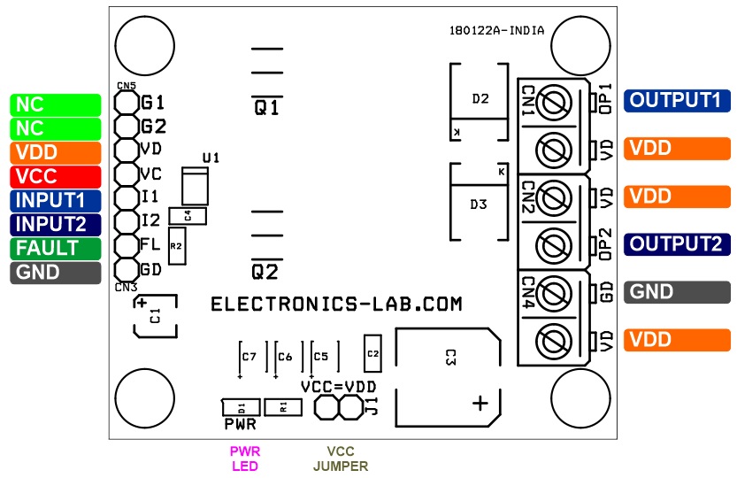
- PCB Dimensions 53.98 x 45.09mm
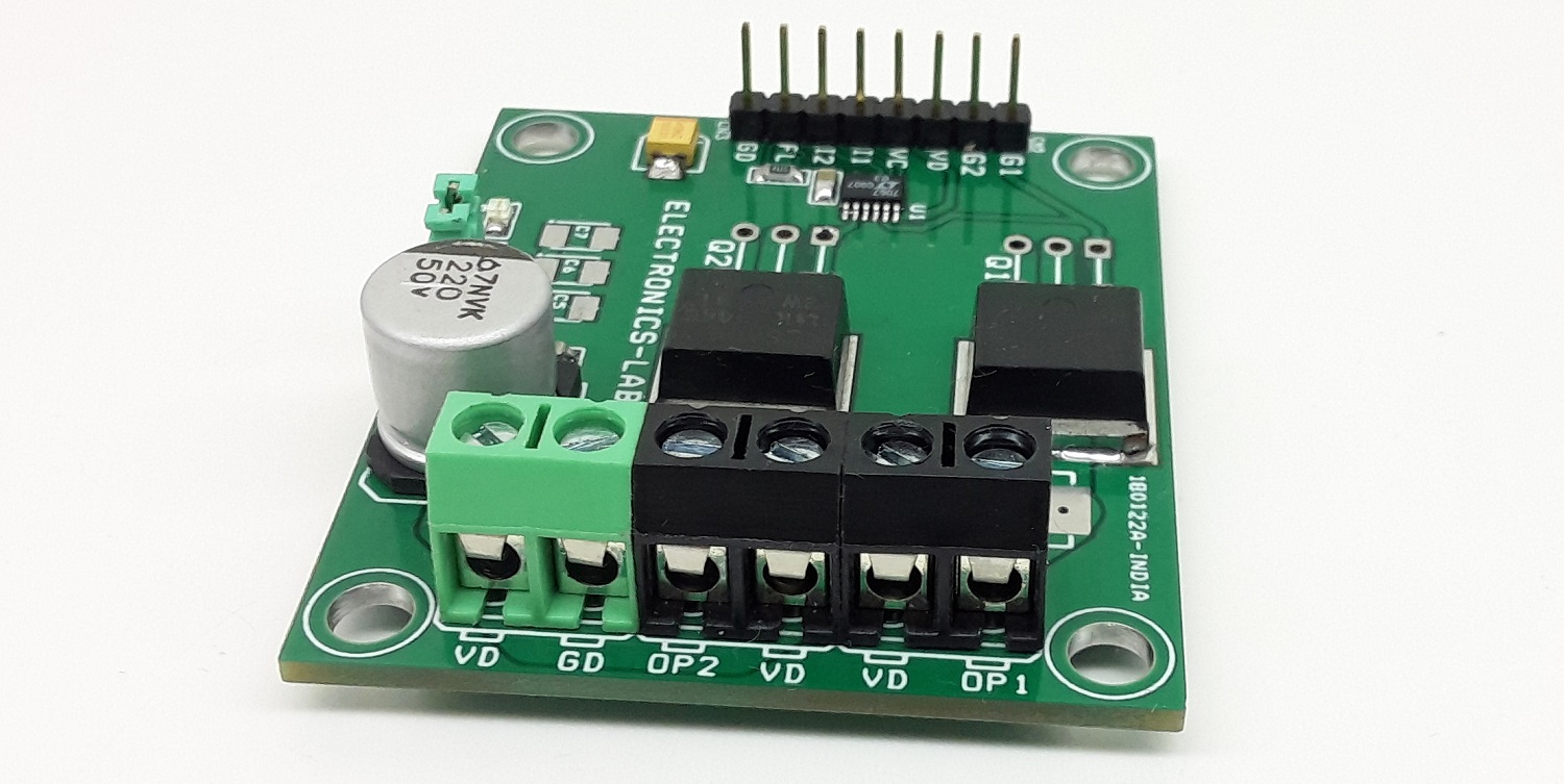
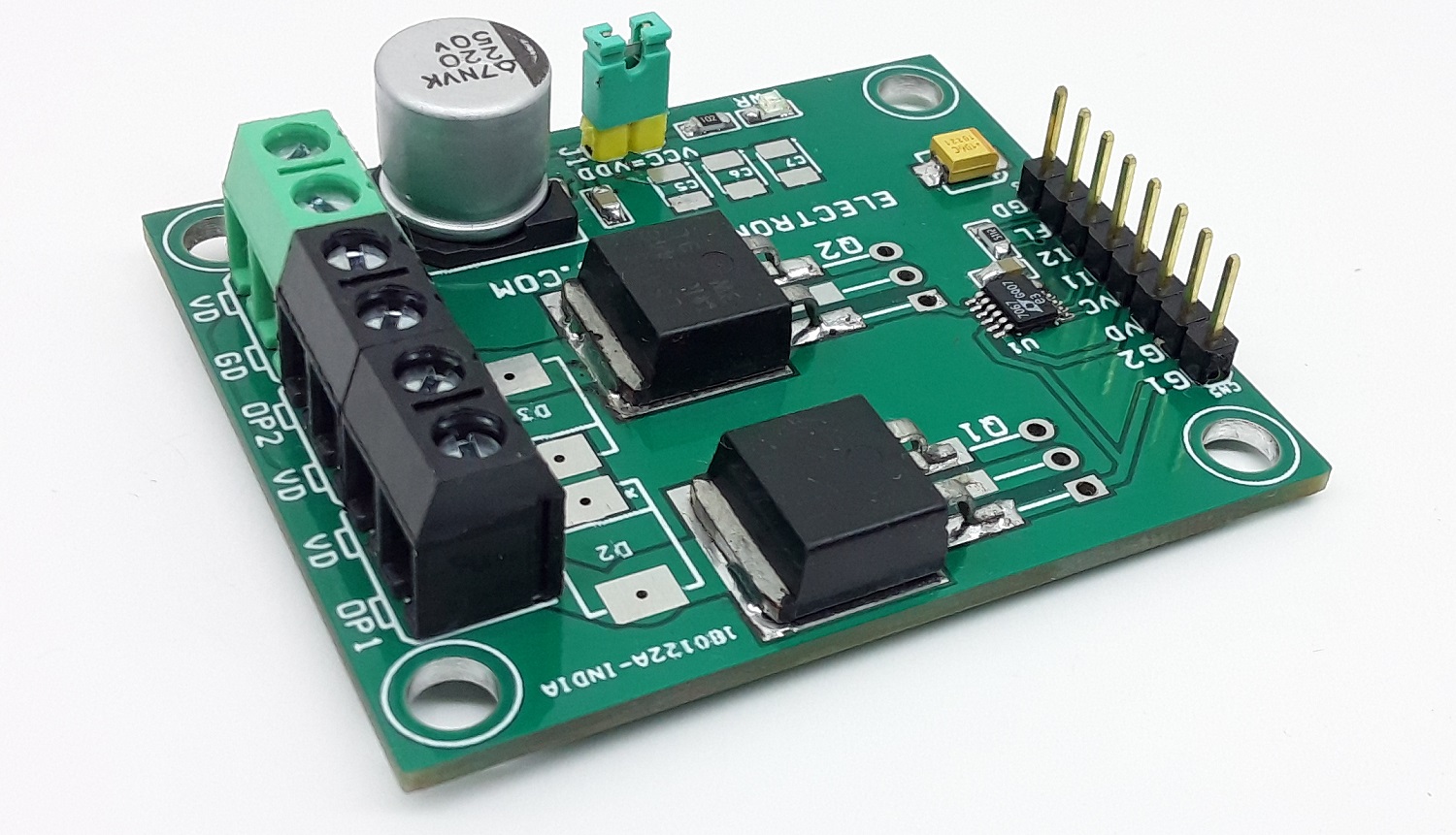
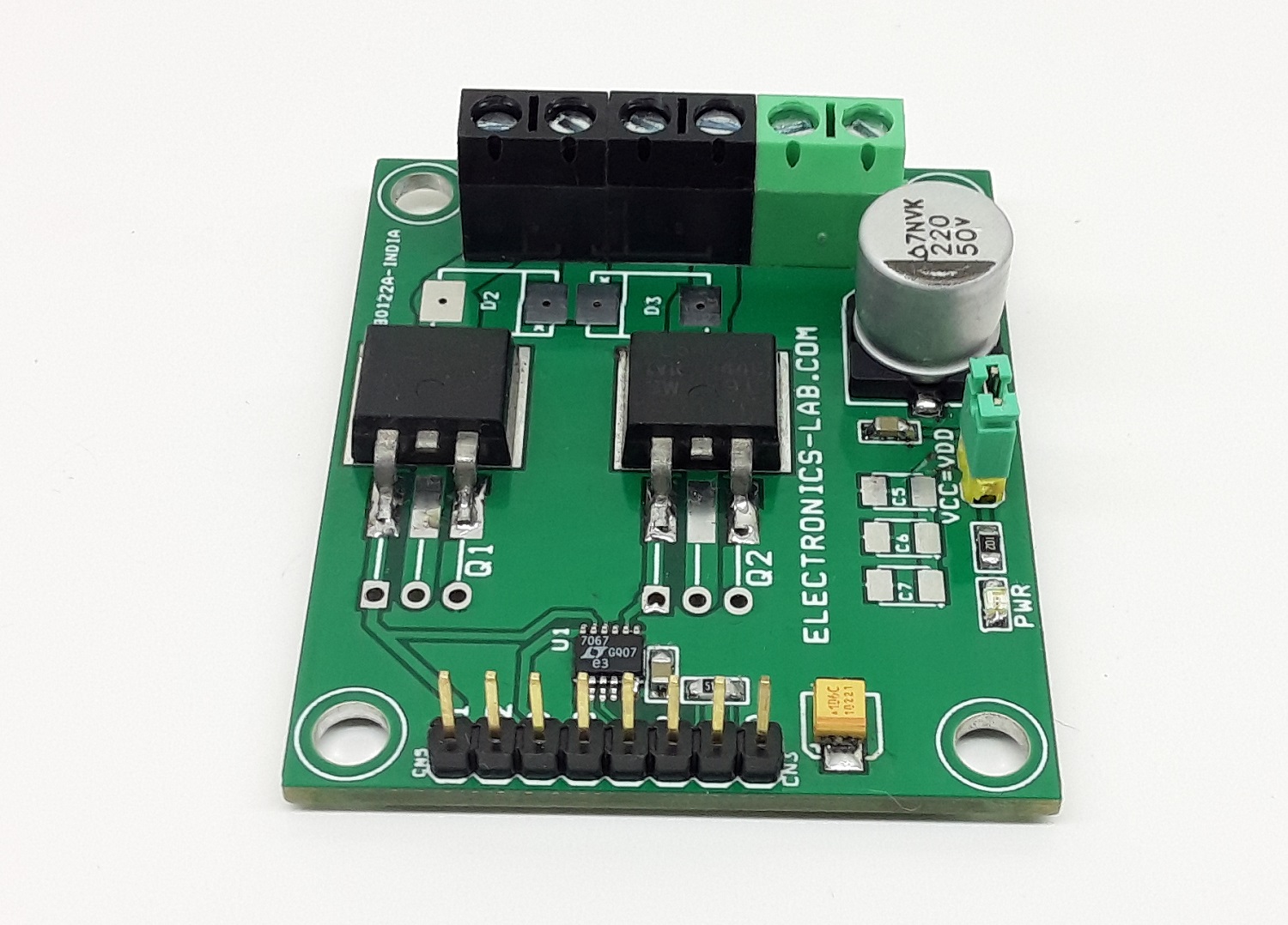
Connections CN3 Connector
- Pin1 VDD Load Supply 12V to 48V
- Pin2 VCC Gate Driver Supply 12V to 14V
- Pin3 Input 1
- Pin4 Input 2
- Pin5 Fault Output Normally High
- Pin6 GND
Other Components Details
- Connector CN1 and CN2 Load 1 and Load2
- Connector CN3 Load Supply 12V to 48V
- LED D1 Power LED
- Jumper J1 for Single Supply Operation (Read Note 1)
- CN5 Not In use
Schematic
Parts List
| NO | QNTY | REF | DESC | MANUFACTURER | SUPPLIER | PART NO |
|---|---|---|---|---|---|---|
| 1 | 2 | CN1,CN2 | 2 PIN SCREW TERMINAL PITCH 5.08MM | PHOENIX | DIGIKEY | 277-1247-ND |
| 2 | 1 | CN3 | 6 PIN MALE HEADER PITCH 2.54MM | WURTH | DIGIKEY | 732-5319-ND |
| 3 | 1 | CN4 | 2 PIN SCREW TERMINAL PITCH 5.08MM | PHOENIX | DIGIKEY | 277-1247-ND |
| 4 | 1 | CN5 | 2 PIN MALE HEADER PITCH 2.54MM | WURTH | DIGIKEY | 732-5315-ND |
| 5 | 1 | C1 | 10uF/16V SMD 1210 OR 1206 | YAGEO/MURATA | DIGIKEY | |
| 6 | 2 | C2,C4 | 0.1uF/50V SMD SIZE 0805 | YAGEO/MURATA | DIGIKEY | |
| 7 | 1 | C3 | 220uF/50V SMD ELKTROLYTIC | WURTH | DIGIKEY | 732-8463-1-ND |
| 8 | 5 | D2,D3,C5,C6,C7 | DNP | READ NOTE | ||
| 9 | 1 | D1 | LED RED SMD SIZE 0805 | LITE ON INC | DIGIKEY | 160-1427-1-ND |
| 10 | 1 | J1 | JUMPER - 2 PIN MALE HEADER PITCH 2.54MM | DIGIKEY | 732-5315-ND | |
| 11 | 2 | Q1,Q2 | IRF540 TO263 | INFINION | DIGIKEY | IRF540NSTRRPBFCT-ND |
| 12 | 1 | R1 | 1K 5% SMD SIZE 0805 | YAGEO/MURATA | DIGIKEY | |
| 13 | 1 | R2 | 51K 1% SMD SIZE 0805 | YAGEO/MURATA | DIGIKEY | |
| 14 | 1 | U1 | LTC7067 | ANALOG DEVICE | DIGIKEY | 505-LTC7067RMSE#PBF-ND |
| 15 | 1 | J1-S | JUMPER SHUNT | SULLINS CONNECTOR | DIGIKEY | S9001-ND |
Connections
Gerber View
Photos