Self-Oscillating Full-Bridge Using IRS2453
This is a Self-oscillating full-bridge project built using the IRS2453 chip. This chip incorporates a high-voltage full-bridge gate driver with a front-end oscillator similar to the industry standard CMOS 555 timer.

This is a Self-oscillating full-bridge project built using the IRS2453 chip. This chip incorporates a high-voltage full-bridge gate driver with a front-end oscillator similar to the industry standard CMOS 555 timer. HVIC and latch-immune CMOS technologies enable ruggedized monolithic construction. The output driver features a high pulse current buffer stage designed for minimum driver cross-conduction. Noise immunity is achieved with a low di/dt peak of the gate drivers and with an under-voltage lockout hysteresis greater than 1.5 V. The IRS2453(1)D also includes latched and non-latched shutdown pins.
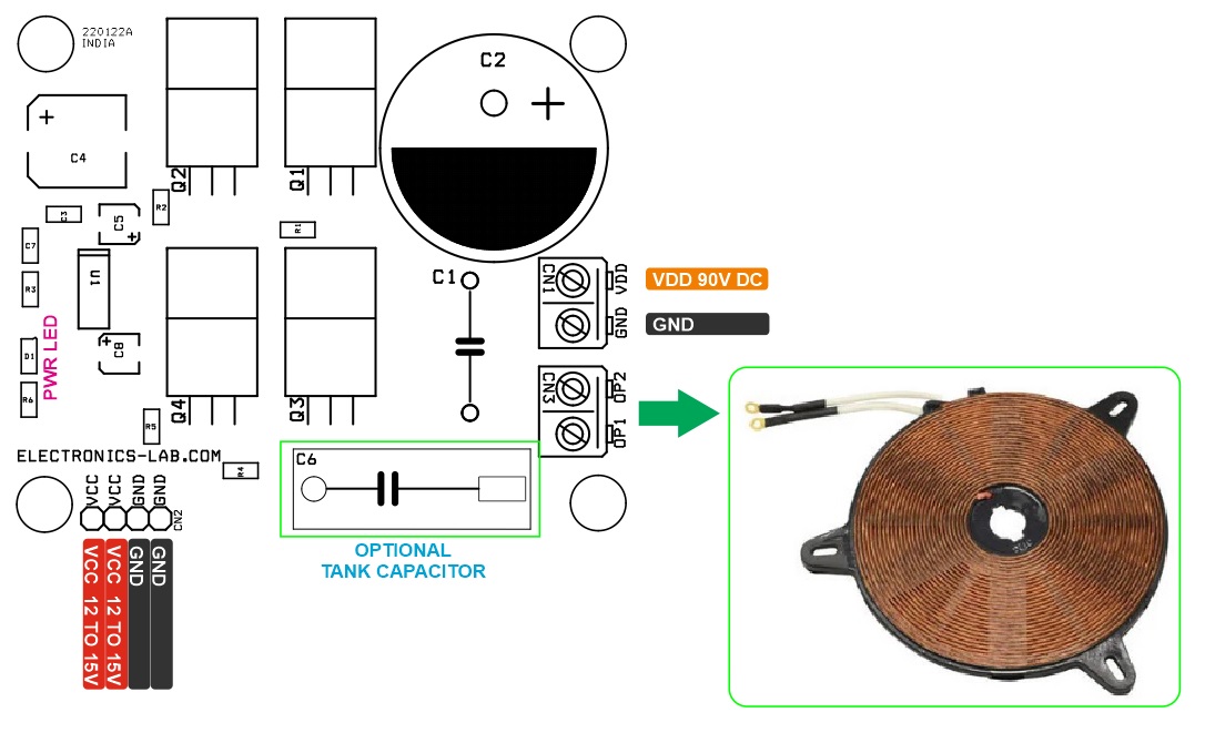
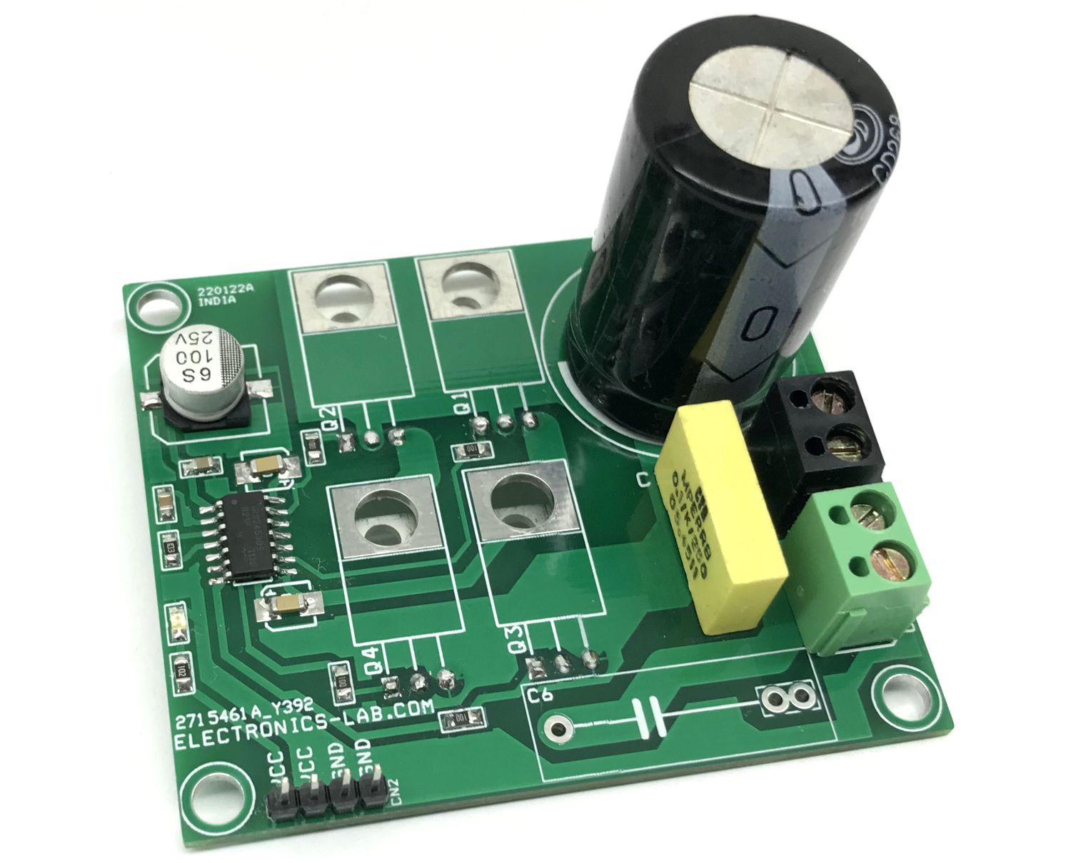
Load Supply voltage: 90V DC, this is limited due to capacitor voltage C1, C2, and MOSFETs Q1-Q4. The board can support DC supply up to 600V, choose appropriate capacitors and MOSFETs.
Oscillator: Refer to the figure below to choose the right value of C7 and R3 to program the oscillating frequency.
Heatsink: Heatsink and Fan are a must for MOSFETs and to dissipate heat.
Features
- Power Supply Gate Driver 12V to 15V DC
- Power Supply 90V Limited by DC Capacitors and MOSFETS (Up to 600V Change Capacitor C1 and C2)
- Frequency 68Khz, Oscillator frequency can be programmed using CT, RT (C7 and R3)
- Load Current Up to 5Amps
- Duty Cycle 50%
- Micropower Startup
- Internal Dead Time 1uS
- 4 x 4 MM Mounting Holes
- PCB Dimensions 69.22 x 58.90 mm
Application
- Wireless Charger
- Low Power DC to AC Inverter
- Tesla Coil
- Induction Heater
Under-Voltage Lock-Out Mode (UVLO)
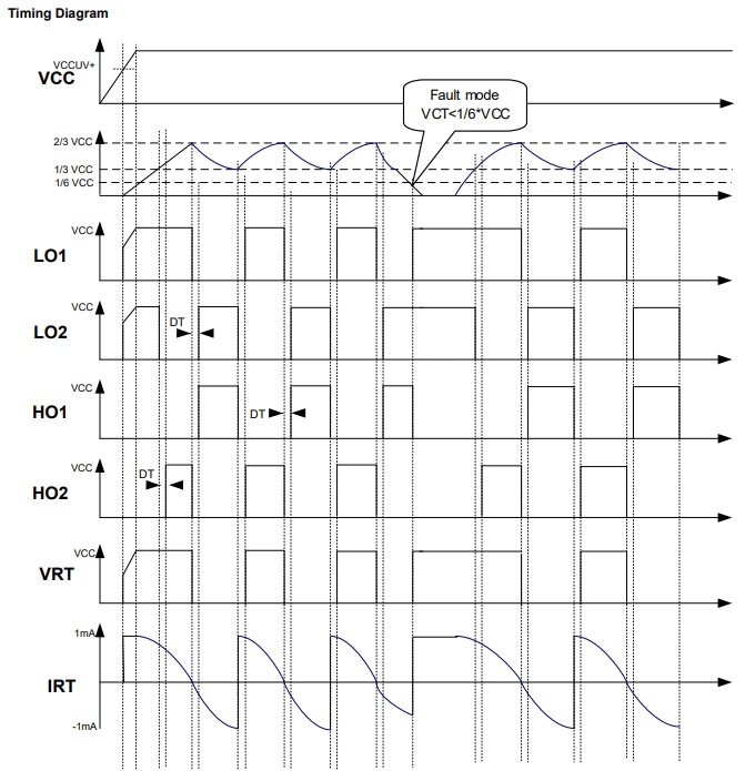
The under-voltage lockout mode (UVLO) is defined as the state the IC is in when VCC is below the turn-on threshold of the IC. The IRS2453(1)D under-voltage lock-out is designed to maintain an ultra-low supply current of e the high and low side output drivers are activated. During under-voltage lock-out mode, the high and low side driver outputs LO1, LO2, HO1, HO2 are all low. With VCC above the VCCUV+ threshold, the IC turns on and the output begin to oscillate.
Normal Operating Mode
Once VCC reaches the start-up threshold VCCUV+, the MOSFET M1 opens, RT increases to approximately VCC (VCC-VRT+) and the external CT capacitor starts charging. Once the CT voltage reaches VCT- (about 1/3 of VCC), established by an internal resistor ladder, LO1 and HO2 turn on with a delay equivalent to the dead time (td). Once the CT voltage reaches VCT+ (approximately 2/3 of VCC), LO1 and HO2 go low, RT goes down to approximately ground (VRT-), the CT capacitor starts discharging and the dead time circuit is activated. At the end of the dead time, LO2 and HO1 go high. Once the CT voltage reaches VCT- , LO2 and HO1 go low, RT goes to high again, the dead time is activated. At the end of the dead time, LO1 and HO2 go high and the cycle starts over again. The frequency is best determined by the graph, Frequency vs. RT, shown below, for different values of CT.
A first-order approximation of the oscillator frequency can also be calculated by the following formula:
f » 1/1.453 x RT x CT
This equation can vary slightly from actual measurements due to internal comparator over- and under-shoot delays
Bootstrap MOSFET The internal bootstrap FET and supply capacitor (CBOOT) comprise the supply voltage for the high-side driver circuitry. The internal bootstrap FET only turns on when the corresponding LO is high. To guarantee that the highside supply is charged up before the first pulse on HO1 and HO2, LO1 and LO2 outputs are both high when CT ramps between zero and 1/3*VCC. LO1 and LO2 are also high when CT is grounded below 1/6*VCC to ensure that the bootstrap capacitor is charged when CT is brought back over 1/3*VCC.
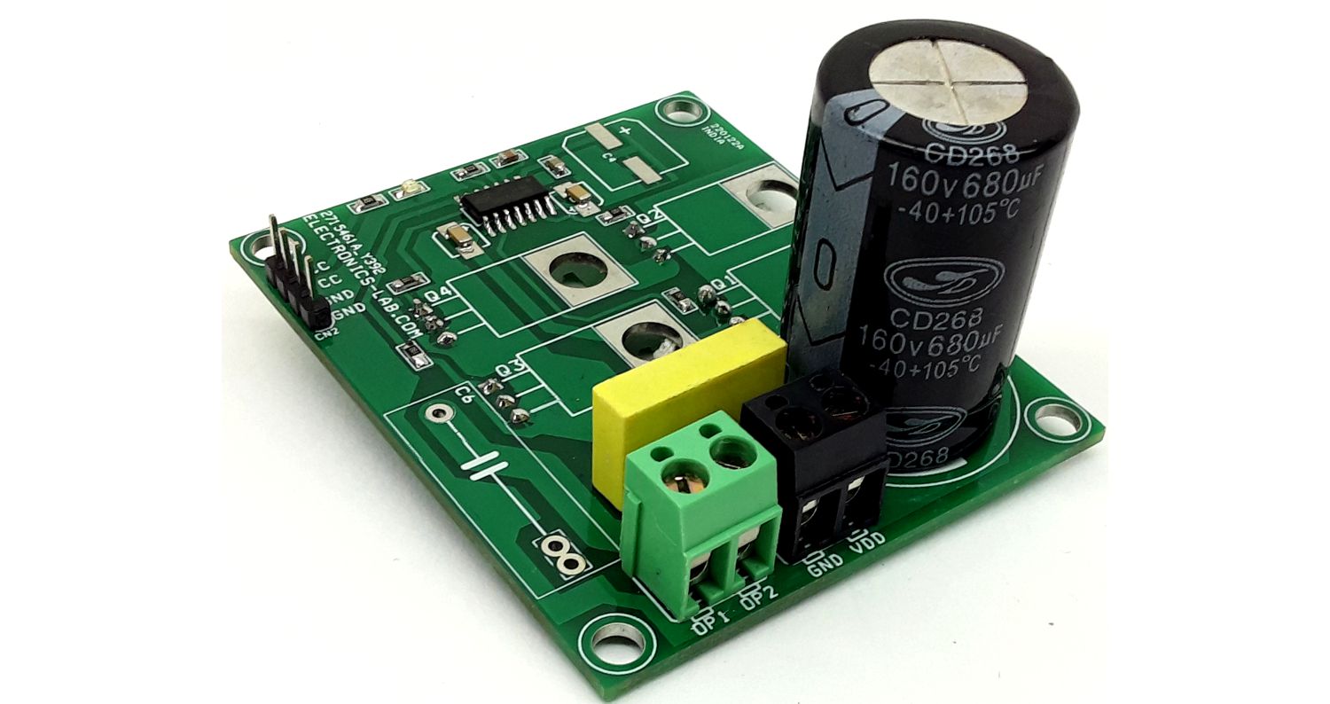
Connections & Other Details
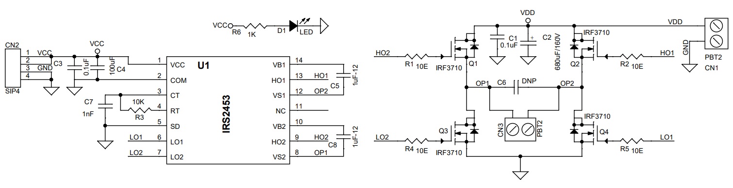
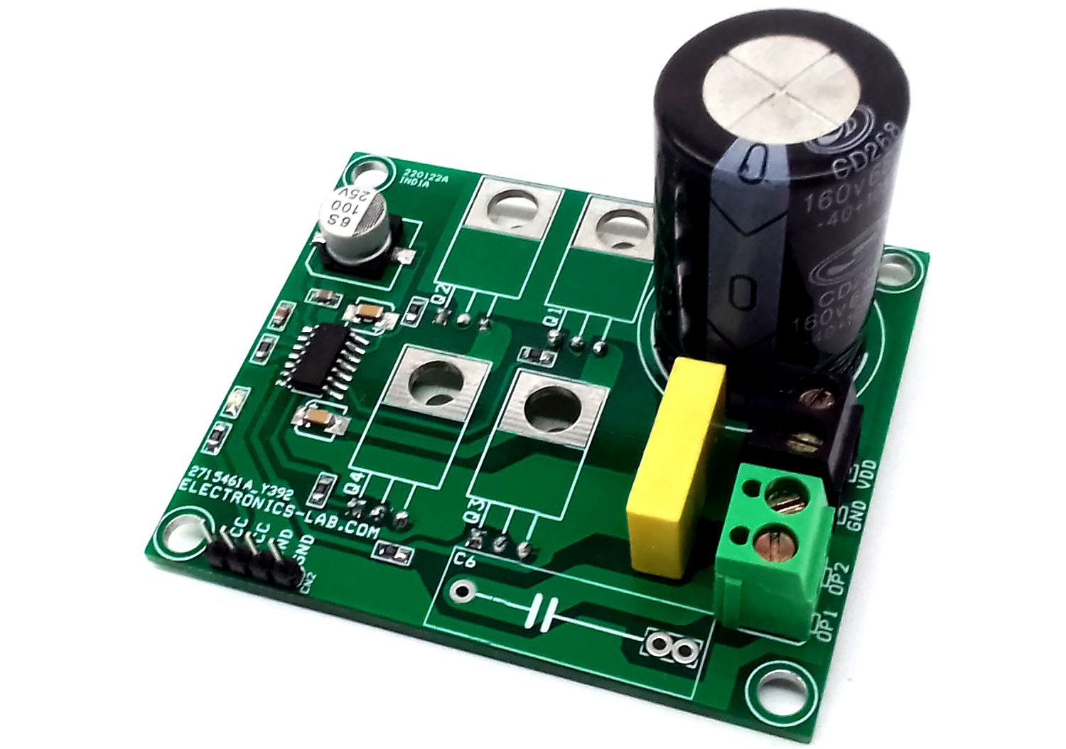
- CN1: VDD Pin 1 = + Load Supply, Pin 2 = GND
- CN2: Pin 1,2 = VCC 12to 15V DC, Pin 2,3 = GND
- D1: Power LED
- R3, C3: Oscillator Programming
Schematic
Parts List
| NO | QNTY | REF | DESC | MANUFACTURER | SUPPLIER | SUPPLIER PART NO |
|---|---|---|---|---|---|---|
| 1 | 2 | CN1,CN3 | 2 PIN SCREW TERMINAL PITCH 5.08MM | PHOENIX | DIGIKEY | 277-1247-ND |
| 2 | 1 | CN2 | 4 PIN MALE HEADER PITCH 2.54MM | WURTH | DIGIKEY | 732-5317-ND |
| 3 | 2 | C1 | 0.1uF/250V -630V | CORNELL | DIGIKEY | 338-3177-ND |
| 4 | 1 | C2 | 680uF/160V | NICHICON | DIGIKEY | 493-2635-ND |
| 5 | 1 | C4 | 100uF/25V ELECTROLYTIC | PANASONIC | DIGIKEY | PCE3797CT-ND |
| 6 | 2 | C5,C8 | 1uF/25V CERAMIC SMD SIZE 1206 | YAGEO/MURATA | DIGIKEY | |
| 7 | 1 | C6 | DNP | READ NOTE | ||
| 8 | 1 | C7 | 1nF/50V CERAMIC SMD SIZE 0805 | YAGEO/MURATA | DIGIKEY | |
| 9 | 1 | D1 | LED RED | LITE ON INC | DIGIKEY | 160-1427-1-ND |
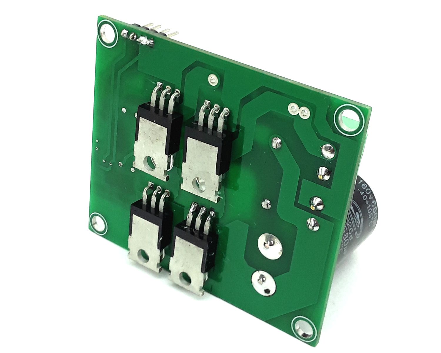
| 10 | 4 | Q1,Q2,Q3,Q4 | IRF3710 MOSFET TO220 | INFINEON | DIGIKEY | IRF3710ZPBF-ND |
| 11 | 4 | R1,R2,R4,R5 | 10E 5% SMD SIZE 0805 | YAGEO/MURATA | DIGIKEY | |
| 12 | 1 | R3 | 10K 5% SMD SIZE 0805 | YAGEO/MURATA | DIGIKEY | |
| 13 | 1 | R6 | 1K 5% SMD SIZE 0805 | YAGEO/MURATA | DIGIKEY | |
| 14 | 1 | U1 | IRS2453 SOIC14 | INFINEON | DIGIKEY | IRS2453DSTRPBFCT-ND |
| 15 | 1 | C3 | 0.1uF/50V CERAMIC SMD SIZE 0805 | YAGEO/MURATA | DIGIKEY |
Connections
Timing Diagram
Frequency Diagram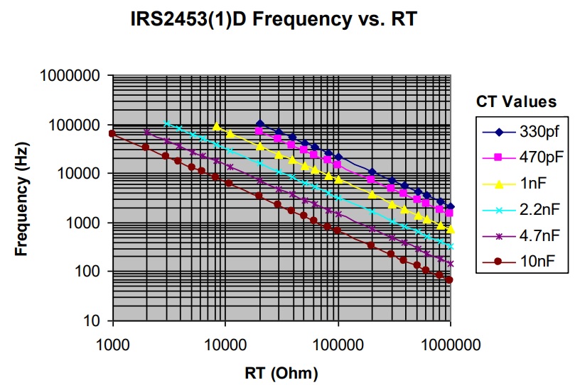
Gerber View
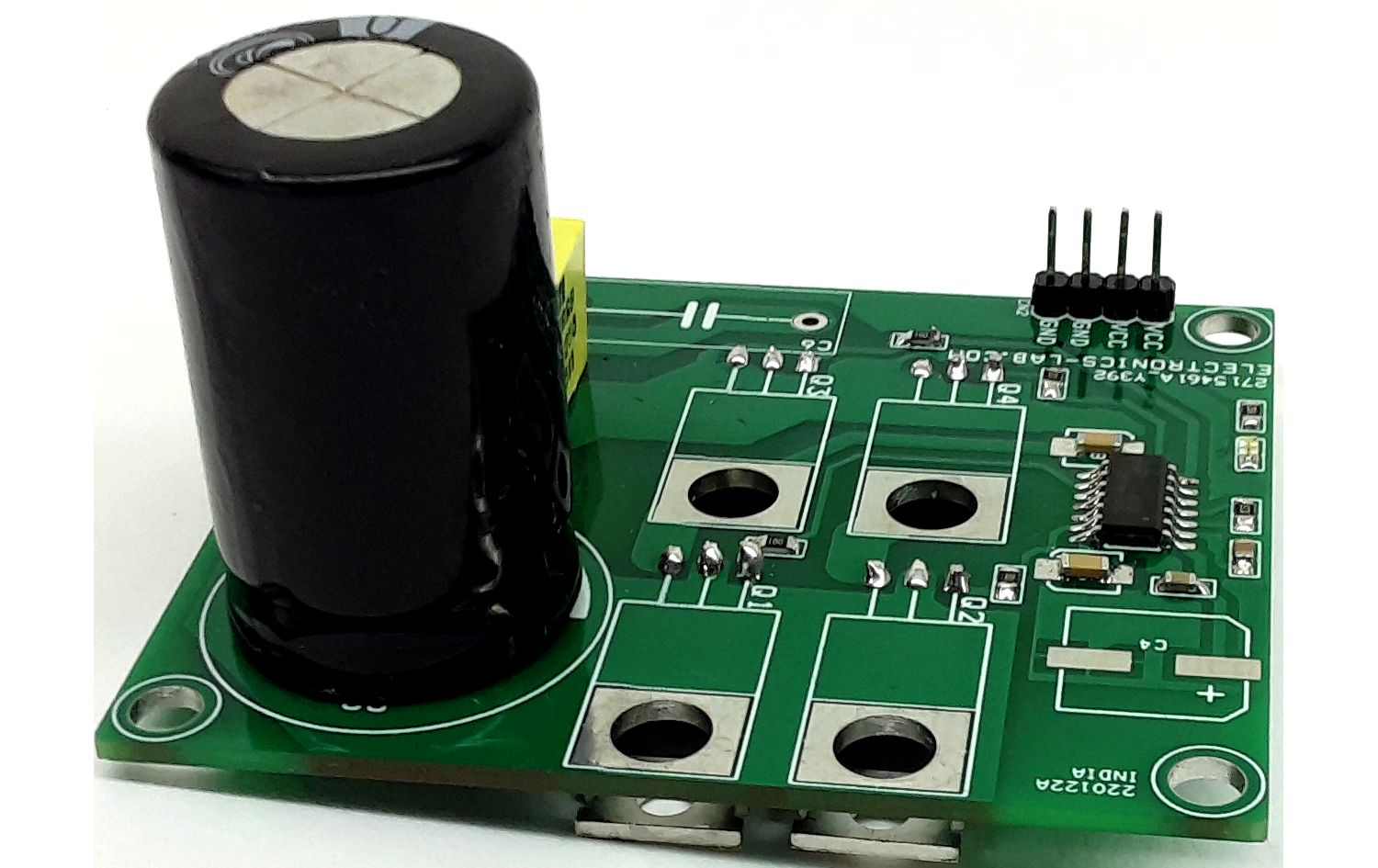
Photos
Can it turn ac to dc