Common Base Amplifier
Presenting the Common Base Amplifier In this article, we present the last topology of amplifiers for bipolar transistors known as the Common Base Amplifier (CBA). In Figure 1 below, the electric diagram of a CBA is presented, no particular bias circuit or decoupling capacitors are shown here.
Presenting the Common Base Amplifier
In this article, we present the last topology of amplifiers for bipolar transistors known as the Common Base Amplifier (CBA). In Figure 1 below, the electric diagram of a CBA is presented, no particular bias circuit or decoupling capacitors are shown here.

Some specifications need to be highlighted for CBAs :
- The base is linked to the ground of the circuit, hence the name “Common Base”.
- The input signal is delivered to the emitter branch of the bipolar transistor.
- The output signal is taken to the collector branch of the bipolar transistor.
Further in the article, we will see that in many ways the CBA behaves in opposition with respect to the Common Collector Amplifier (CCA).
Equivalent circuit
An equivalent circuit of Figure 1 can be drawn considering the collector branch to be an ideal current source and the p/n junction between the collector and emitter branches to behave like a small diode resistance re=25 mV/Iout.
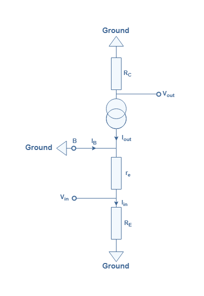
It can already be anticipated from Figure 2 that since Iin=Iout+IB (from Kirchhoff’s laws), the current gain AI=Iout/Iin of a CBA configuration is AI=1-(IB/Iout)<1. Therefore, the current gain of a CBA configuration is strictly lower than 1, so this type of amplifier cannot amplify currents. However, we will see further in the tutorial that the voltage gain is high.
Current gain
We have already seen in the previous paragraph that the current gain AI is strictly lower than one. To get the exact formula of Ai, we consider as mentioned previously that Iin=Iout+IB. Moreover, we define Iout=β×IB with β the transistor’s current gain. Notice that here IB≠Iout in contrary to the previous amplifier configurations CEA and CCA.
The output current satisfies Iout=AI×Iin=β×IB , when isolating AI, it comes :
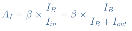
Dividing the numerator and denominator by IB, the term Iout/IB=β appears and we get the exact expression of the current gain for a CBA configuration :
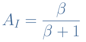
As an example, a bipolar transistor of gain β=200 has a current gain AI=200/201=0.995≅1. Hence, the current gain of a CBA configuration can always be approximated by 1 without committing too much error. Since the current gain is equal to 1, the output current Iout follows the input current Iin, hence the other name commonly given to this configuration current follower/buffer.
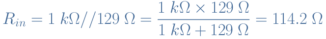
Input resistance
As seen from the input in the emitter branch, the total input resistance is RE//re where the symbol “//” denotes the fact that the emitter and small diode resistor are in parallel.
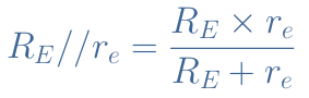
However, the emitter resistance RE is always much higher than the small diode resistance re, hence it comes :
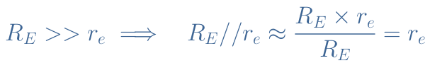
The input resistance of a CBA configuration is therefore equal to the small diode resistance re between the emitter and collector branches, this value of impedance is very small.
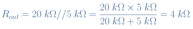
Output resistance
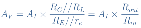
On a real CBA configuration, a load RL is placed in parallel with the collector resistance RC. The output resistance is thus given by Rout=RC//RL. If the load is chosen such as RL>>RC, the output resistance simplifies to Rout=RC.
Voltage gain
It is considered in the following, such as proved previously that AI≅1. The voltage gain of a CBA configuration is thus given by the ratio AV=Vout/Vin where Vout=RC×Iout and Vin=(RE//re)×Iin. It comes afterwards that :
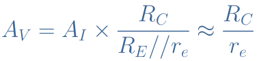
Since the collector resistance satisfies RC>>re, the voltage gain of a CBA configuration is very high. We can moreover highlight that the voltage gain of a CBA configuration is the same as for Common Emitter Amplifiers except that the sign is here positive : the output voltage signal is in phase with the input voltage signal. This formula is valid if the load RL is considered to satisfy RL>>RC. However, in the general case, the expression of the voltage gain is :
Example : Voltage, Current and Power gains
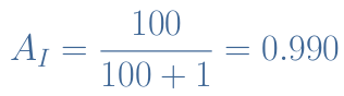
In this section, we consider a real CBA configuration presented in Figure 3 with a voltage divider network to bias the base which is composed of two resistor R1 and R2. Moreover, a load RL is in parallel with the collector resistance RC. Notice that a decoupling capacitor is added between the base and ground to make this diagram correct, but for the sake of simplicity, its value is not given and won’t be taken into account for the following calculations. Finally, the bipolar transistor’s current gain is β=100.

The current gain of this CBA configuration is simply given by :
Before determining the voltage gain of this configuration, the first step is to calculate the total input and output resistances, and for that, we need the value of the small diode resistance.
The voltage drop in the collector resistance RC is given by :

Therefore, the current across the collector resistance is IC=VC/RC=0.97 V/5 kΩ=194 μA. From this value, it comes that the small diode resistance is re=25 mV/194 μA=129 Ω.
The input resistance is hence given by :
Since in this configuration RL<RC, the parallel resistance RL//RC needs to be considered as the total output resistance :
Finally, the voltage gain is determined from Equation 4 :
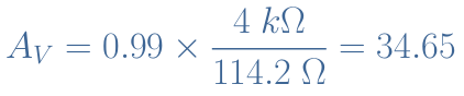
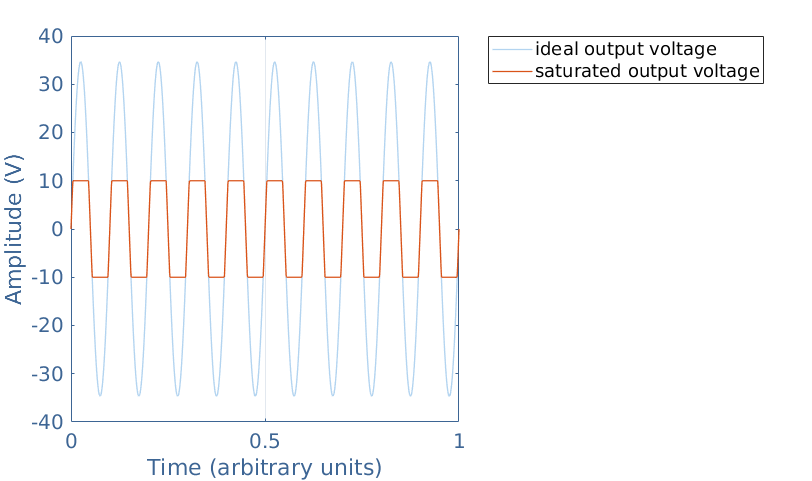
In theory, the voltage can here be amplified by a factor 34.65. However, as seen during the Introduction to Electronic Amplifiers tutorial, the output voltage is limited by the power supply votage. Therefore, the output voltage here reaches only 2×Vsupply=20 V peak to peak instead of 2×34.65=69.3 V peak to peak and a rather important saturation effect will be observed.
It is interesting to check if our calculations are correct in determining both input and output currents :
- The input current is given by Vin/Rin=1 V/114.2 Ω, thus Iin=8.76 mA.
- The output current is given by Vout/Rout=34.65 V/4 kΩ, thus Iout=8.66 mA.
We can see that the input and output currents are approximately equal and the ratio Iout/Iin=0.99 gives again the current gain previously calculated.
If we consider that the output voltage can indeed be amplified by a factor 34.65, the power gain AP of this configuration is given by AI×AV=0.99×34.65, thus AP=34.3. However, since RL=4×RC, only a fourth of the power is delivered to the load : AP,load=8.57.
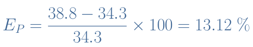
Using the simplified expression from Equation 3 RC/re=5 kΩ/129 Ω gives a voltage gain AV=38.8. The simplified value of the current gain is AI=1 which in turn gives a power gain AP=38.8 instead of 34.3 for the real value. The error EP for the power gain is therefore :
Conclusion
In this tutorial, we dealt with many aspects of one of the three elementary topology of amplifier known as the Common Base Amplifier (CBA). We have seen that such a configuration cannot amplify currents since its current gain is approximately equal and strictly lower than 1, hence the name “current buffer/follower” often given to CBAs. However, we have seen through theory and an example that the voltage signal can be highly amplified and its voltage gain is only limited by the power supplied in the collector branch. As opposition to the Common Collector Amplifier, the input resistance of a CBA configuration is low and its output impedance is high. This feature makes CBAs very useful to interpose between low load inputs and high load outputs such as in radio frequency circuits. Finally, we have seen through an example how to practically calculate the voltage, current and power gains of a CBA configuration.
As a general conclusion, we have seen during this tutorial three elementary configurations of bipolar transistor-based amplifier : the Common Emitter Amplifier (CEA), the Common Collector Amplifier (CCA) and the Common Base Amplifier.
We summarize and give in the following a comparison of these different configurations:
- In absolute value, the voltage gain is the same for CEA and CBA configurations. However the CEA shifts the signal of a 180° phase since it has a sign “-“, therefore, the CEA inverts the signal.
- The input resistance is : approximately the same for CEA and CCA configurations.
- The output resistance is : the same for CEA and CBA configurations.
- The voltage gain is : high for CEA and CBA, ≅1 for CCA.
- The current gain is : high for CEA and CCA, ≅1 for CBA.
- The power gain is : very high for CEA, high for CBA, medium for CCA.
Finally, due to their different characteristics, the applications of these three configurations are also different :
- The CEA, due to its high voltage and current gains is used as a universal amplifier.
- The CCA, due to its high input and low output resistances is used as a step-down impedance adapter. It is also used as a current amplifier and an oscillator.
- The CBA, due to its low input and high output resistances is used as a step-up impedance adapter. It is also used as a voltage amplifier, an oscillator or a high frequency amplifier thanks to its good behavior in frequency.


Fig 1 can’t be right. Vsupply is shorted to ground.
Yes, right. Thansk for noticing. We updated the figure.