Phase Splitter
Introduction Often, not only the amplitude of the signal is interesting to transform, such as amplifiers do, but also its phase. Bipolar transistors can indeed be used in the design of a device called a phase splitter.
Introduction
Often, not only the amplitude of the signal is interesting to transform, such as amplifiers do, but also its phase. Bipolar transistors can indeed be used in the design of a device called a phase splitter.
In the very first section, general notions about the phase and the properties of a phase splitter are given, so we understand the context. The second section will present the architecture of a phase inverter based on the design of a common emitter and common collector amplifiers.
Not only BJT transistors can be used to make phase splitters, but we will see in a third section that a more interesting phase splitter can be designed with operational amplifiers (OA). Moreover, we detail a particular case of OA-based phase splitter in a next section that can be used to make a phase modulator.
General concepts and presentation of the phase splitter
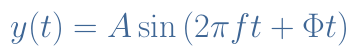
Any periodic signal has three important parameters that fully define it : the amplitude A, the frequency f and the phase Φ. A sinusoidal signal y(t) can for example be written such as shown in Equation 1 :
The value of the phase dictates the value of y(t=0). Actually, the value of the phase of a signal is not important and does not have any impact on the signal itself. As an example, if you listen to an audio signal, you will never distinguish the difference between a 0° or 90° phase signal.
Moreover, without having access to initial conditions or a reference, it can not be measured : the same thing happens with the electric potentials. However, such as for electric potentials, a phase shift or phase difference can be measured between two signals and this value is useful.
Let’s consider two sine signals that have the same frequency but different phases Φ1 and Φ2. The phase shift φ is a constant value and it is simply defined by φ=Φ1-Φ2. If we consider a reference signal of phase Φr=0°, three notable phase shifts can be highlighted as shown in Figure 1 :
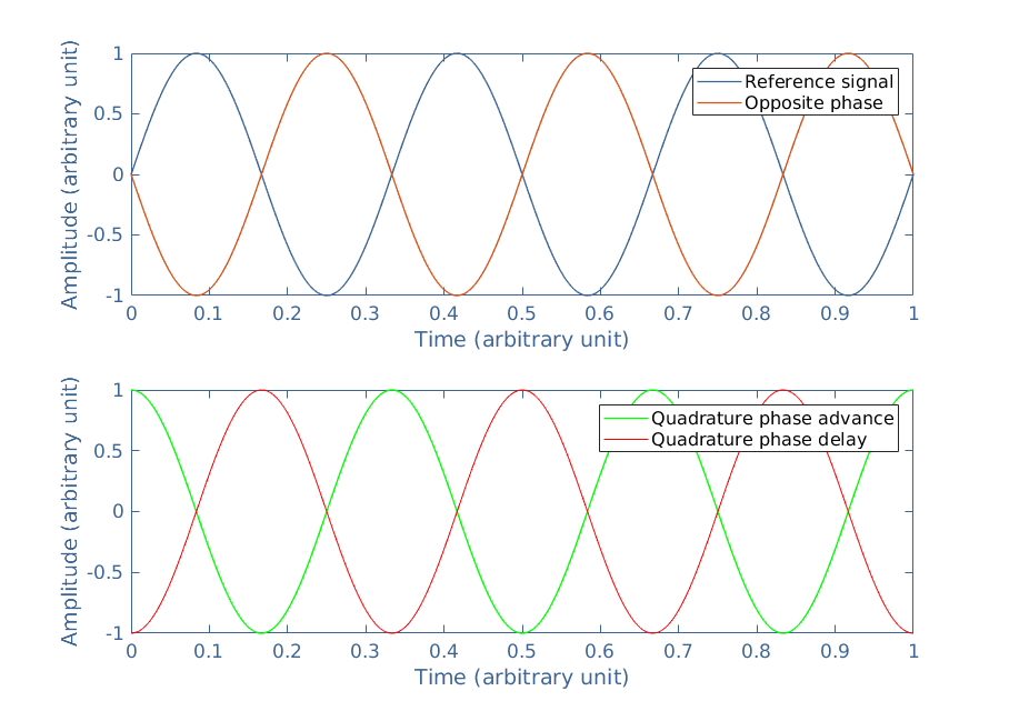
An opposition phase is shifted of 180° or π rad with respect to the reference signal. Quadrature phases are shifted of +90° or +π/2 rad for the phase advance and –90° or -π/2 rad for the phase delay.
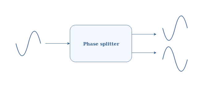
Most of the time, the goal of phase splitters is to generate two outputs : one reference and an opposition or quadrature phase shifted signal. During this operation, no amplification of the signal is necessary and phase splitters usually have a unit gain to only modify the phase.
BJT-based phase splitter
A phase inverter, that is to say a phase splitter that shifts the signals of 180° can be built with combining a common emitter and a common collector amplifiers. The architecture of the BJT-based phase splitter is shown in the Figure 3 :
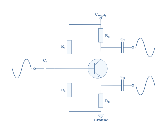
We recognize in this figure the emitter-follower structure wired to the emitter branch and the common emitter structure wired to the collector branch. Let’s analyze separately how these two architecture works, the reader should not hesitate to refer to the Common Emitter and Common Collector (emitter-follower) tutorials for the following.
Concerning the common emitter part of this design (RC and C2), the voltage gain is equal to -RC/RE. By setting RC=RE, the voltage gain becomes -1 so that the first output signal conserve the same amplitude as the input but with its phase inverted. This signal is commonly known as the inverting output.
For the emitter-follow part (RE and C3), the voltage gain is intrinsically equal to +1. The output is therefore conserving the same amplitude and phase as the input. This signal is known as the non-inverting output.
Operational amplifier-based phase splitter
A phase splitter can also be designed with an operational amplifier (OA) and a potentiometer. The advantage of this configuration is that, unlike the BJT-based phase splitter where the phase is only inverted, it can here vary from 0° to almost 360°.
We distinguish two setups for an OA-based phase splitter : the delay and advance phase splitters. In Figure 4 below, the architecture of a delay phase splitter is presented :

By applying Millman’s theorem, we can show that the transfer function T(f) of this circuit is given by the following formula :
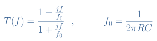
The delay phase splitter respects that the gain of the signal is equal to 1. Indeed we can note that the numerator of T(f) is a complex number and its denominator is the conjugate complex of the numerator. Since the module of the complex conjugate is equal to the module of the same complex number, the module of T(f) is equal to 1.
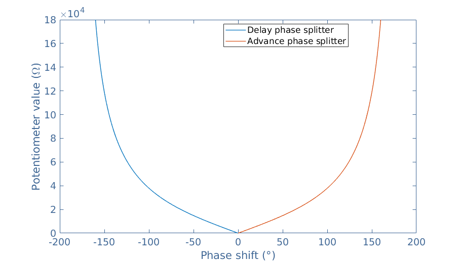
Moreover, the evolution of the phase Φ(f) with the frequency is given by Arg(T(f)) which is the argument of the transfer function. It can be shown that Φ(f,RP)=-2Arctan(2πRPCf), the phase is therefore directly influenced by the value of the potentiometer RP. We can note that in the case of the delay phase splitter, the phase shift is negative and for a potentiometer that can vary such as shown in Figure 4, the value is between -160° and 0°.
Positive phase shifts can be accessed with an advance phase splitter, its architecture shown in Figure 5 is slightly different :

In this case, the phase shift is expressed just as for the delay phase splitter but with an opposite sign : Φ(f,RP)=+2Arctan(2πRPCf).
When combining the circuits of Figure 4 and 5 in cascade (in serie), a large range of phase shifts can be accessed as shown in the following graph :
Phase modulator
Having understood how an OA-based phase splitter works, we can now design a very useful device called a phase modulator performing phase modulation (PM). A PM consists of transforming the phase of a carrier signal in order to be able to transmit information.
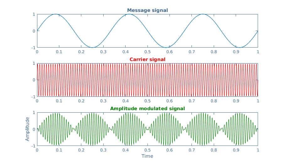
The most visual modulation technique is the amplitude modulation (AM) and represented in Figure 7. It consists in multiplying the message signal (low frequency) with a carrier signal (high frequency fc). The message is contained in the envelope of the modulated signal and can be recovered by using low-pass filters.
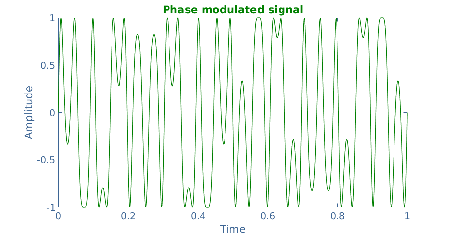
In PM technique, instead of modulating the amplitude, we modulate the phase. Unlike for the AM technique, it is not very visual and easy to estimate how the original message signal looks like by only observing the phase modulated signal :
A phase modulator can be built by modifying the OA-based phase splitter. The capacitor is replaced by a field effect transistor (MOSFET) which gate is controlled by the carrier signal such as shown in Figure 9.

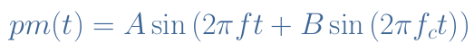
Mathematically, originally the message signal is of the form such as shown in Equation 1. The phase modulator circuit of Figure 9 transforms the signal such as the phase modulated signal pm(t) contains a function phase Φ(t) instead of a constant phase and is of the form presented in Equation 3 :
Conclusion
Phase transformation is another great function that BJT and OA-based amplifiers can perform. Phase shifting has many applications among which phase modulation and balanced topology drivers (driving push-pull configurations for example) are the most known.
In the first section of this tutorial, we have clearly defined what are the phase and the phase shift. This last one is an important property that gives the temporal spacing between two signals. A phase shift can be from -180° to +180° which represents the point where the two signal are in opposition. The -90° and +90° values are called quadrature shifts and it is important to know how to shift two signals from such values since some important applications (wireless LAN for example) use this property.
The first circuit we have presented, is capable of performing phase splitting, and is a combination of common emitter and common collector amplifiers. We have seen that this configuration can provide two outputs : one identical to the input and one phase inverted signal. It is a simple design and the phase shift is constant and cannot be modified by an external command.
In the next section, we have presented an operational amplifier (OA) based phase splitter that can overcome the constant phase shift problem of the BJT-based phase splitter. We have indeed seen that depending on the position of the capacitor in the circuit, an advance or delay phase splitter can be made by combining the use of a variable resistance. This circuit enables to obtain a the full range of phase shifting possible between -180° and +180° if the variable resistance can reach a high enough value.
Finally, in the last section we have proposed a modified version of the OA-based phase splitter in order to design a phase modulator. This architecture includes a MOSFET connected to the non-inverting terminal of the OA that is controlled by a carrier signal. This phase modulator performs a phase modulation which is one of the techniques along with the amplitude (AM) and frequency modulation (FM) that are used in telecommunications.


Hello, for the FET phase splitter, are the output amplitudes same as the original input amplitude or HALF that? There is a video on YouTube that states that for and FET phase splitter, with same resistors on the source and drain, the output signals amplitude is half that of the input. I believe that this is wrong. Hope to hear from you. Thanks.