Digital to Analogue Converter (DAC)
Digital-to-Analogue Converter (Binary Weighted) The Digital-to-Analogue Converter (DAC) are opposite of the Analogue-to-Digital Converter. It employs a method by which binary digital signals are transformed into analogue signals.
Digital-to-Analogue Converter (Binary Weighted)
The Digital-to-Analogue Converter (DAC) are opposite of the Analogue-to-Digital Converter. It employs a method by which binary digital signals are transformed into analogue signals. With its output (voltage or current) proportionate to the value of its digital input number, DACs transform binary or non-binary numbers and codes into analogue ones.
Conversion of digital to analogue (DAC) is a method by which binary digital signals are transformed into analogue signals, which have an endless number of possible states. For example, a 4-bit digital logic circuit converts 00002 to 11112 (F0 to F15), wherein a voltage output ranging from 0 to 10V is produced by the DAC.
There are several ways to convert an “n”-bit digital input code into an equivalent analogue output voltage between 0 and some VMAX value, but the most popular and simple conversion techniques use an operational amplifier and a resistor ladder network, or weighted resistors and a summing amplifier.
The weights determined by the resistive values employed in the ladder networks provide a varied “weighted” amount to the signals generated in both digital-to-analogue conversion methods, which result in a weighted sum output.
Operational Amplifiers
Negative feedback reduces and controls the extremely high open-loop gain (AOL) of operational amplifiers, for this purpose inverting op-amp circuit is used. A tiny portion of the output signal is sent back to the input terminal to accomplish this.
The input voltage VIN of the amplifier is linked directly to its inverting input through an appropriate input resistor RIN. The closed-loop voltage gain, AV(CL), of an inverting amplifier is given by the ratio of these two resistors, as indicated.
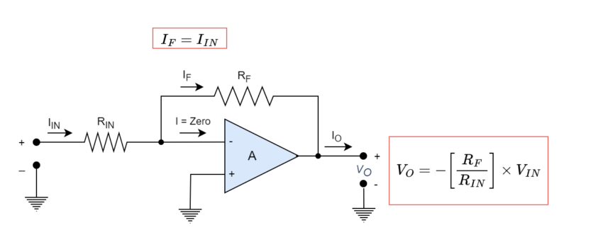
From the above fig, we see that VO is calculated by multiplying VIN by the closed-loop Gain (ACL), which is based on the input resistance (RIN) divided by the feedback resistance (RF). Therefore, we may modify the closed-loop gain of the op-amp and, the value of VO (IF*RF) for a given input signal by adjusting the values of either RF or RIN.
Digital-to-Analogue Converter (Summing Amplifiers)
The aforementioned instance of an inverting operational amplifier uses a single input voltage signal. However, what would happen to the circuit and its gain if we introduced another input resistor for combining two or more analogue signals into a single output?
The single input circuit above may be changed into a summing amplifier, or more specifically, a “summing inverting voltage amplifier” circuit, by connecting numerous inputs to the operational amplifier’s negative end.
Any input signals are essentially electrically separated from one another because the feedback resistor’s RF negative feedback sets the op-amp’s inverting input at zero potential. The output, then, is the inverted sum of all the input signals. As a result, when a summing amplifier is in the inverting mode, it generates the negative sum of all input voltages, but when it is not inverting, it generates the positive output. Examine the circuit below.
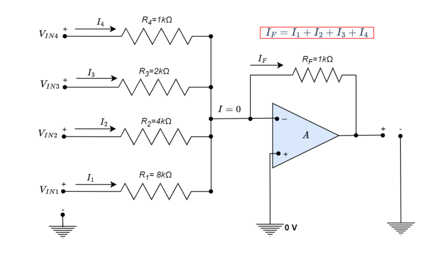
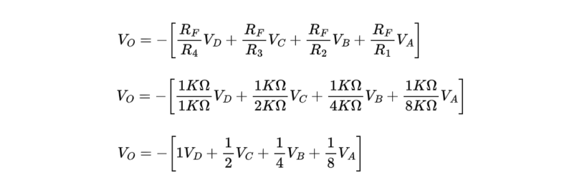
We may adjust the initial equation for the inverting amplifier arrangement above to account for these four additional input values as follows: In the summing amplifier circuit above, the output voltage (VO) is proportional to the sum of the four input voltages, VIN1, VIN2, VIN3, and VIN4.
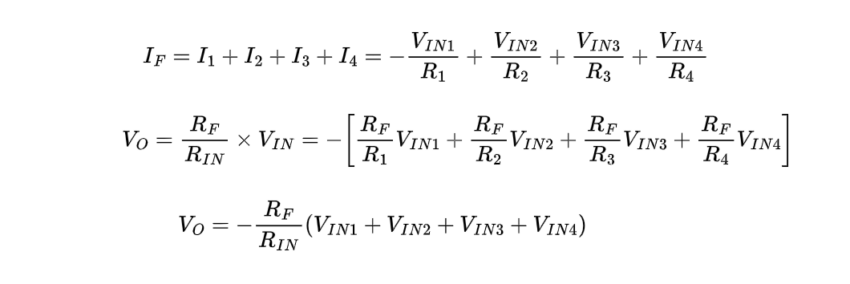
Then, when each input voltage is multiplied by its matching gain and added to the subsequent one to get the total output, we can see that the output voltage is an inverted, scaled sum of the four input voltages.
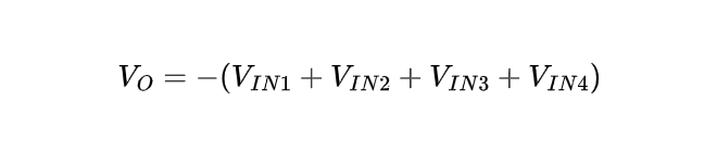
Each input channel will have a closed-loop voltage gain of unity (1) if all the resistances are the same and have similar values, that is, RF = R1 = R2 = R3 = R4. As a result, the output voltage can be found easily by the mentioned equation:
Digital-to-Analogue Converter (4-Bit Binary Weighted)
A 4-bit binary weighted digital-to-analogue converter can be created by assuming that the four inputs of the summing amplifier are binary inputs with voltage values of either 0 or 5 volts (“Low-0” and “High-1”) and by doubling the resistive values of each input resistor to the previous one. This will result in an output condition that would be the weighted sum of these four input voltages.
With the four input resistors ranging from 1kΩ to 8kΩ (or multiples thereof), we may build a straightforward 4-bit binary weighted analogue-to-digital converter circuit as illustrated by labelling the four summing inputs as A, B, C, and D and setting RF = 1kΩ.
There are 24 = 16 possible combinations for a 4-bit binary number, ranging from 00002 to 11112. 8-4-2-1 is the binary coding ratio that results from doubling the weight of each input bit to the previous one.
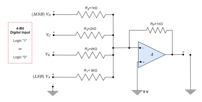
The transfer characteristic of the 4-bit binary weighted digital-to-analogue converter would therefore be as follows if we set the input resistances for “D” at 1kΩ, “C” at 2kΩ (i.e., the double of D), “B” at 4kΩ (double of C), and “A” at 8kΩ (double of B), with the feedback resistance (RF) set at 1kΩ as shown in the figure above,
If we apply a TTL voltage of +5 volts (logic “1”) to the summing amplifier’s input VD, which represents the most significant bit (MSB), we see that the gain of the op-amp will be RF/R4 = 1kΩ/1kΩ = 1 (unity) VD, Therefore, the output of the digital-to-analogue converter circuit will be -5 volts when a 4-bit binary code of 1000 is applied.
Similarly, if the input VC of the summing amplifier receives +5 volts (logic 1), the gain of the op-amp is equal to RF/R3 = 1kΩ/2kΩ = 1/2 (one-half). Therefore, the analogue output voltage of -2.5 volts would be produced by the 4-bit binary code 0100.
When Logic “1” is applied to the VB, the gain of the amplifier will be RF/R2 = 1kΩ/4kΩ = ¼ (one-fourth). Hence, the 4-bit binary code of 0010 will produce an output voltage of -1.25 volts.
Ultimately, when logic “1” is applied to the least significant bit (LSB) input of the summing amplifier VA, It would result in an output voltage of -0.625 volts (a 12.5% resolution) and RF/R1 = 1kΩ/8kΩ = 1/8 (one-eighth) with the 4-bit binary code of 0001.
The mentioned table will give the detailed result of VO when +5 volts is applied to 4-bit binary weighted analogue-to-digital converter.
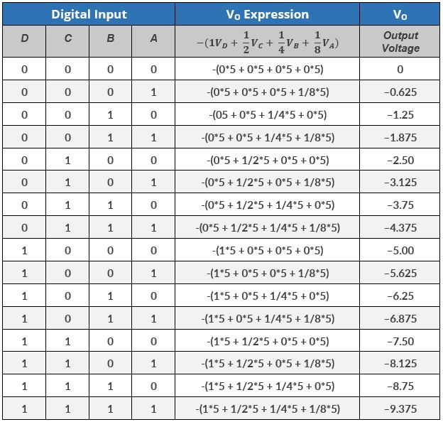
From the above values, we observed that, for each bit changed, there would be a difference of 0.625 volts.
The resolution of the analogue output voltage for a binary-weighted digital-to-analogue converter may be enhanced by increasing the number of binary digits and the resistive summing network such that each resistor has a separate weighting.
For instance, an 8-bit DAC with +5 input volts; will produce (1/128)*5 = 0.0039, similarly, a 12-bit DAC will result in (1/2048)*5 = 0.0024 volts per change in the input binary code.
The downside here is that for a “n”-bit DAC, a binary weighted resistor DAC necessitates a wide range of high precision resistors (one per bit), which makes it unfeasible (and costly) for converters with higher resolution than a few bits.
But by transforming it into an R-2R resistor ladder DAC, which only needs two precise resistance values—R and 2R—we may build on the concept of a binary weighted digital-to-analogue circuit arrangement that employs variable value resistors. We will examine how the R-2R Digital-to-Analogue Converter transforms a digital binary number into an analogue voltage output using just two resistor values in the upcoming update about digital-to-analogue converters.
Conclusion
- The Digital-to-Analog Converter (DAC) translates digital data in binary format into analogue signals, such as voltage or current, based on the value of its digital input number.
- Inverting Operational Amplifier Circuit is used for the conversion of digital signals to analogue ones. Negative feedback lowers and regulates the operational amplifiers’ extraordinarily high open-loop gain (AOL).
- The closed-loop Gain (ACL) is derived by dividing input resistance (RIN) by the feedback resistance (RF). The output Voltage VO is calculated by multiplying the input voltage VIN and Gain (ACL).
- The “Summing Inverting Voltage Amplifier” circuit is used for multiple inputs; inputs are connected to the negative end of the operational amplifier, herein the output voltage (VO) is proportional to the sum of all the input voltages.
- The transfer characteristic of the 4-bit binary weighted digital-to-analogue converter with +5 volts input, with the feedback resistance (RF) set at 1kΩ, 8-4-2-1 binary weighted DACs will provide an output voltage change of 0.625 volts for each bit that is modified.
- The drawback is that a binary weighted resistor DAC for a “n”-bit DAC requires a large range of high precision resistors (one per bit), which renders it impractical (and expensive) for converters with resolutions of more than a few bits. We use R-2R resistor ladder DAC for high resolution.


