Transmission Gate
Transmission Gate A transmission gate is a form of a bilateral switch constructed using Metal Oxide Field Effect Transistors (MOSFETs) that can be externally controlled through logic levels. A switch, analog one to be precise, controls the passage of analog signals through it and is a type of solid-state semiconductor device.
Transmission Gate
A transmission gate is a form of a bilateral switch constructed using Metal Oxide Field Effect Transistors (MOSFETs) that can be externally controlled through logic levels. A switch, analog one to be precise, controls the passage of analog signals through it and is a type of solid-state semiconductor device. The control of these analog switches is processed using digital logic signals. These analog switches are commercially available in different configurations & forms and can be utilized as a transmission gate. These solid-state semiconductor analog switches resemble conventional electromechanical contacts e.g. Normally Close (NC), Normally (NO), Single Pole Single Throw (SPST), and Single Pole Double Throw (SPDT), etc.
The electromechanical relays are quite tedious due to being costly, spacious, and more importantly, their high operating time. Contrary to this, a solid-state switch is made using Metal Oxide Semiconductor (MOS) which makes it superior in terms of operating time, is relatively cheaper and small. A solid-state switch can transmit a signal current through it depending on the logic levels at its control input. One such bilateral switch, CMOS 4016B, is commonly available in the market.
Like other semiconductor devices, Metal Oxide Semiconductor (MOS) devices comprise N-type MOS (NMOS) and P-type MOS (PMOS) devices and can perform logical switching functions. A digital circuit can be deployed to control this logical switching and depending on the type of device, logic levels lead to different operating conditions such as closed or open conditions. A type of solid-state semiconductor switch that allows transmission of signal or data in either direction (both ways) is referred to as a Transmission Gate (TG) and to understand its working principle, it is essential to consider the operation of a Field Effect Transistor (FET) as a basic analog switch.
Solid-state Analog Switch
A simple controlled single-pole switch can be constructed using a Bipolar Junction Transistor (BJT) or a Field Effect Transistor (FET). In terms of construction, a Metal Oxide Semiconductor FET (MOSFET) has an additional layer of metal between the gate terminal and main conducting channel compared to bipolar devices. Additionally, its main conducting channel is purely resistive in characteristics.
The MOSFET as a Switch
In the following figures, the MOSFET’s basic N-channel and P-channel configurations as a switch have been shown.
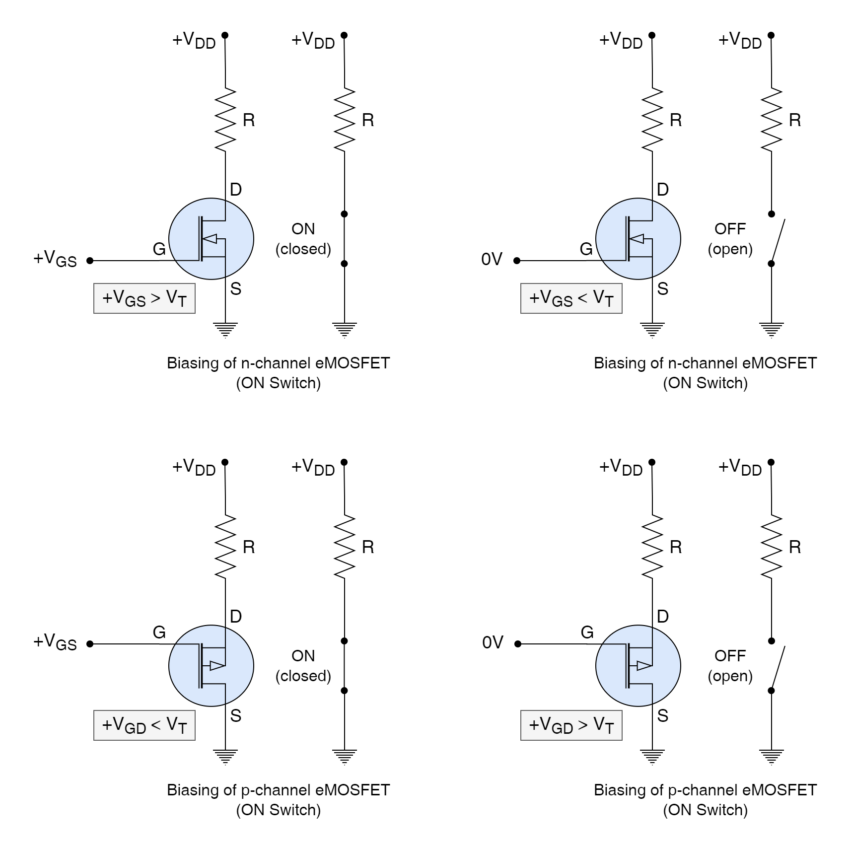
From the above figures, it is observed that certain conditions are required in order to achieve illustrated switching conditions of n-channel (NMOS) and p-channel (PMOS) devices. These conditions refer to a “Threshold Voltage” (VTH) which is the minimum voltage required at the Gate Terminal to initiate conduction in the main conducting channel between source and drain. For an n-channel MOSFET to behave as a closed switch, the VGS (gate-source voltage) must be greater than the VTH (threshold voltage) i.e. VGS > VTH. Whereas, an n-channel MOSFET acts as an open switch when VGS (gate-source voltage) is less than the VTH (threshold voltage) i.e. VGS < VTH. Similarly, a p-channel MOSFET behaves as a closed switch when VGD (gate-drain voltage) is less than the VTH (threshold voltage) i.e. VGD < VTH and it acts as an open switch when VGD (gate-drain voltage) is greater than the VTH (threshold voltage) i.e. VGD > VTH.
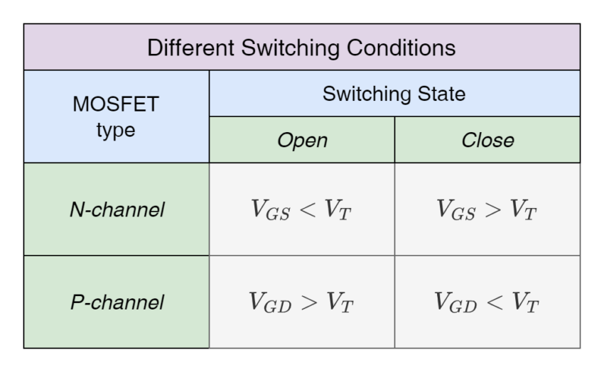
The conditions mentioned above required for each switch condition are illustrated in the following table.
The enhancement MOSFET or eMOSFET is commonly used as a switching device that operates in cut-off (OFF state/ open) and saturation regions (ON state/ close). So, VGS (gate-source voltage) or VGD (gate-drain voltage) is controlling voltage to toggle between the OFF or ON state of an enhancement MOSFET.
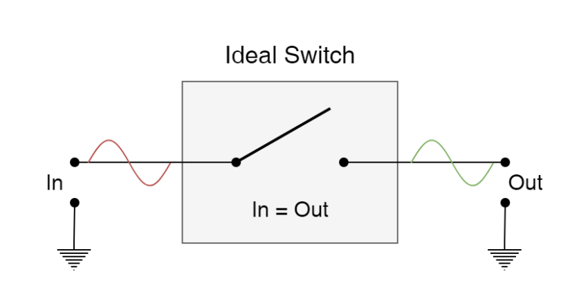
Ideal Switch
The ideal switch is a lossless device somewhat similar to a mechanical switch i.e. it creates a short-circuit in the closed position and an open circuit during open state. Ideally, the signal at input appears at output without any alteration, and an ideal analog switch is shown in the following figure.
However, solid-state switches are not perfect and prone to losses and leakages at different states of operations. These solid-state switches have “ON” state resistances (RON), ranging up to several ohms, causing power losses (I2R) in the form of heat. Whilst their “OFF” state resistances are in kilo-ohms and, as such, they allow passage of a negligible amount of current (Pico amperes) in the main channel. Despite these, enhancement MOSFET is the most widely used switching device that can be effectively controlled by a control voltage applied at its “Gate” terminal.
The NMOS Switch as an Analog Switch
An n-channel MOS device allows transmission of analog signals when the input signal is connected to the “Drain” terminal whereas the control signal is applied at the “Gate” terminal. Once the “ON” condition is met, the input signal appears at the output i.e. “Source” terminal. In the following figure, an n-channel MOS (NMOS) along with its block diagram is shown.
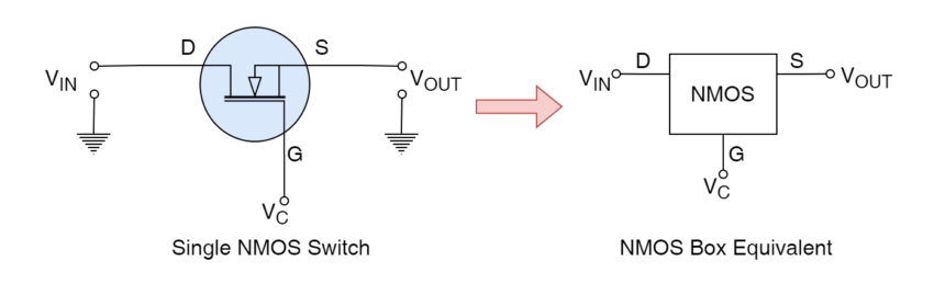
When input (VIN) and output (VOUT) are connected to the “Drain” and “Source” terminals, respectively, the control input (VC) determines the conduction state of its main channel connecting the “Drain” and “Source” terminals.
When the control voltage (VC) is at LOW state (zero voltage) then NMOS will be in the cut-off region as the “Gate” terminal voltage is not positive with respect to the “Drain” and “Source” terminals. In cut-off operation mode, the conduction path of its main channel remains open and no signal passes from input to output as the “Drain” & “Source” terminals are isolated.
If the control voltage (VC) at “Gate” becomes positive (+) then it turns “ON” the conduction channel of the NMOS device and is said to be operating in the saturation region. This state of the NMOS device resembles the closed state of a switch. In addition, when the “Drain” voltage is more positive compared to the “Gate” terminal, the current flows in the main channel from the “Drain” to “Source” terminals which connects the input (VIN) and output (VOUT) terminals.
However, if input voltage (VIN) becomes zero whilst control voltage (VC) is positive then the main channel becomes open and no current flows through it leading to zero drain-to-source voltage (VDS).
In a nutshell, an NMOS device passes the input signal present at the “Drain” terminal towards its “Source” terminal (output) as long as the control voltage (VC) is HIGH and the NMOS device stops passing the signal to the output, otherwise. The control voltage (VC) is the deciding input for the open and close position of the NMOS device. However, it is important that control voltage (VC) with respect to the source i.e. VGS (gate-to-source voltage) must be kept significantly higher compared to the specific threshold voltage (VTH) of that NMOS device otherwise significant voltage drop and loss will occur at the conduction channel (drain-to-source). As such, an NMOS device is known to pass a weak “HIGH” signal and a strong “LOW” signal through it.
The PMOS Switch as an Analog Switch
The working of p-channel MOS (PMOS) is similar to the NMOS device described above, however, there are some minor differences. In PMOS, the direction of current is from source to drain rather than from drain to source in the case of an NMOS device. Moreover, input and output signals are connected to “Source” and “Drain” terminals, respectively, as shown in the following figure.

When a control voltage (VC) of zero magnitude is applied at the “Gate” terminal of the PMOS device and is more negative compared to “Source” & “Drain” inputs then the PMOS device will be operating in the saturation region (closed or ON state). If the “Source” voltage is positive and greater than the applied control voltage (VC) then the current (ID) will flow from the “Source” to the “Drain” terminal which connects the input with the output terminal.
When the input voltage (VIN) at the “Source” terminal is set to zero and, on the other hand, the control voltage (VC) is kept at zero or below zero (negative) voltage then the main conduction channel remains open leading to no current flow state with source-to-drain voltage (VDS) at zero potential gradient. In such a case, input and output terminals are isolated.
When a positive control voltage (+VC) is applied at the “Gate” terminal then the conduction channel of PMOS becomes “OFF” similar to an open-circuit condition and the PMOS transistor is said to be operating in the cut-off region. In this state, no source-to-drain current (ID) flows in the main channel and the input is isolated from the output terminal.
In brief, control voltage (VC) determines the state of the PMOS transistor. When VC is at zero or below zero (negative) potential then the PMOS transistor is operating in the saturation region and conduction between input and output terminals is established (ON state). Whereas, a positive or “HIGH” state input at the “Gate” terminal (VC), sets the operation of the PMOS device in the cut-off region and no conduction occurs between input & output terminals (OFF State).
In PMOS transistors, it is important to keep gate-to-source voltage (VGS) significantly less compared to the Threshold Voltage (VT) of the PMOS transistor enabling it to turn OFF completely otherwise the current will still flow in the conduction channel. Therefore, a PMOS transistor is said to pass a strong “HIGH” signal and a weak “LOW” signal through its channel. On the contrary, as seen above, an NMOS transistor exhibits passing a strong “LOW signal and a weak “HIGH” signal. Thus, looking at the characteristics of NMOS & PMOS devices, it is possible to pass both “LOW” and “HIGH” logics strongly in either direction by combining these MOS devices and this forms the basis of a Transmission Gate.
Transmission Gate
Transmission Gate is a basic bilateral switch formed by connecting NMOS and PMOS devices together in parallel. This parallel symmetry enables bilateral operation i.e. input and output are interchangeable. This CMOS switch has been shown in the following figure by superimposing triangles pointing in opposite directions.
The configuration shows the placement of NMOS and PMOS devices in a reverse parallel configuration with an inverter at the input of the “Gate” terminal of the PMOS device to ensure the presence of opposite (complementary) control voltages at the “Gate” terminal of each device. When the control voltage is at “LOW” logic then both NMOS and PMOS devices are in cut-off states and the Transmission Gate opens to isolate input & output. Likewise, when the control voltage is set to a “HIGH” state then both devices are biased into saturation mode, and the Transmission Gate closes to conduct. Therefore, a Transmission Gate is closed when VC = 1 and starts conducting current from either direction whereas it isolates input & output when VC = 0.
Truth Table and Boolean Expression of a Transmission Gate
Likewise, in other logic gates, a Transmission Gate’s function can be defined using either a Truth Table or a Boolean expression. In the following figure, a Truth Table has been shown of a Transmission Gate along with its symbol.
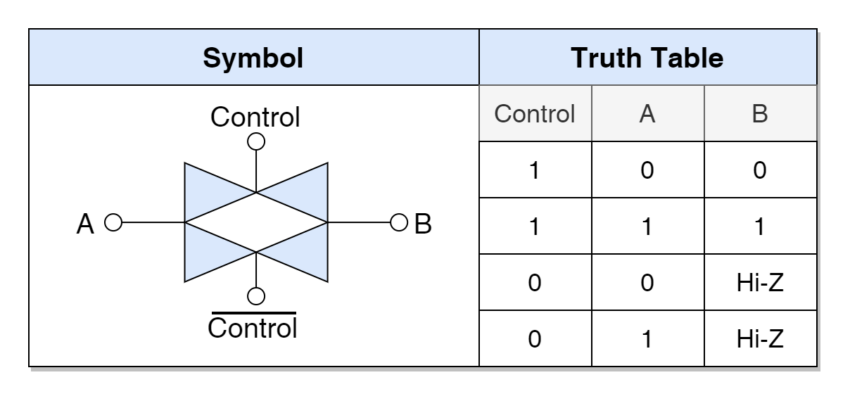
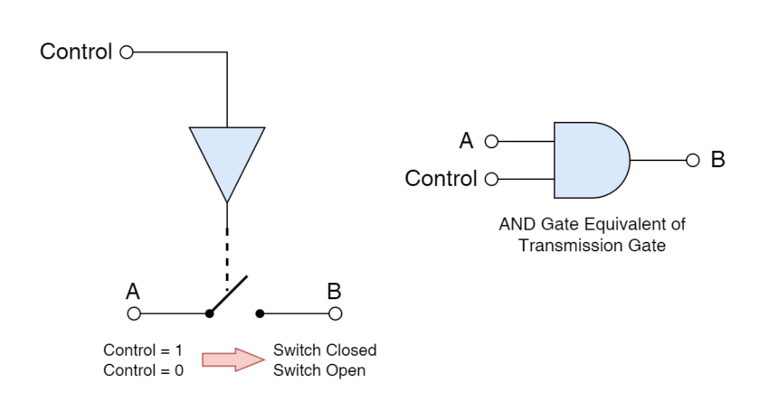
It is evident from the Truth Table that the output function of “B” is dependent on both inputs i.e. “A” & “Control”. However, output at the “B” terminal is always “Hi-Z” irrespective of the “A” terminal input as long as “Control” is set to “0”. This resembles an AND operation of inputs “A” & “Control” which eventually yields a Boolean expression of a Transmission Gate as defined below:

The Boolean expression requires a 2-input standard AND gate with inputs “A” and “Control” as operands to implement it as shown in the following figure.
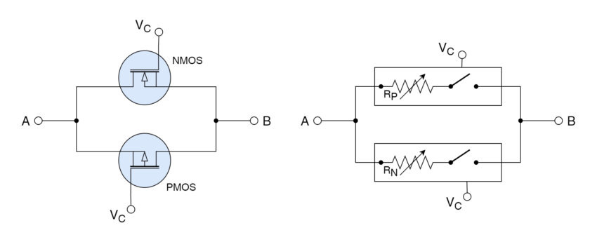
As shown earlier, each of these MOS devices can independently act as a switching device and presents an On-resistance (RON) during conduction. However, their parallel configuration in the form of a Transmission Gate effectively reduces the On-resistance (RON) during the conduction even though either of the MOS devices conducts depending on the direction of current or input & output selection. Whilst, a non-conducting MOS device, presents a several thousand ohmic resistance but overall parallel On-resistance (RON) effect of conducting and non-conducting MOS devices remains quite low compared to the On-resistance (RON) of an individual device. This is demonstrated using the following figure.
Conclusion
- An ideal analog switch is a lossless switch somewhat identical to a mechanical switch. It creates a short circuit, having nearly zero resistance, when closed and open-circuited by physically isolating input and output terminals.
- A solid-state switch is small, cost-effective, and very responsive to switching operations. Their states are controlled through an additional input using a “Control” signal. However, it has some losses associated with each of its switching states. In a closed state, it has a specific On-resistance (RON) causing I2R losses in form heat and carries a leakage current in the open state as well.
- A Metal Oxide Semiconductor Field Effect Transistor (MOSFET) can also act as a switching device besides a Bipolar Junction Transistor (BJT) and offers several advantages over BJT switches.
- An n-channel MOS device has input and output signals connected to “Drain” and “Source” terminals, respectively. It conducts when the Control Voltage is set to “HIGH” and conduction stops when it is set to “LOW” state. An NMOS device is a good transmitter of “LOW” signals and a poor transmitter of “HIGH” signals.
- A p-channel MOS device has input and output signals connected to “Source” and “Drain” terminals, respectively. It does not conduct when the Control Voltage is set to “HIGH” and starts conducting when it is set to “LOW” state. A PMOS device is a good transmitter of “HIGH” signals and a poor transmitter of “LOW” signals.
- A Transmission Gate is a bilateral switch formed by combining NMOS and PMOS devices in a reverse parallel configuration and, as such, holds the characteristics of both NMOS and PMOS devices i.e. it is a good transmitter of both “LOW” and “HIGH” states.
- A Transmission Gate acts as a closed switch when the Control Voltage (VC) is set to “HIGH” and as an open-circuit when the VC is set to a “LOW” state. Moreover, it presents a lower On-resistance (RON) compared to individual MOS devices acting as a switch.


messed up p mos in the beginning