Bus Transceiver
Bus Transceiver A Transceiver is a device allowing a bidirectional interface between buses for either digital or analog signal communication and has input & output control capability. It uses back-to-back Tri-state buffers for the communication of multiple devices over a common data bus.
Bus Transceiver
A Transceiver is a device allowing a bidirectional interface between buses for either digital or analog signal communication and has input & output control capability. It uses back-to-back Tri-state buffers for the communication of multiple devices over a common data bus. Contrary to a Digital Buffer, a Tri-state Buffer allows bidirectional communication and the ability to control its output by using an additional “Enable” input.
In a unidirectional interface, a device can either transmit or receive and, as such, an additional unidirectional interface will be required for transmit or receive purposes. A bidirectional interface allows devices to transmit and receive. The word “Transceiver” is the amalgamation of words taken from transmitter and receiver. Transceivers are also commonly known as driver/ receiver or send/ receive devices.
As discussed in the Digital Buffer article, unlike other logic gates, a Digital Buffer does not perform inversion or decision-making in a logic circuit. It outputs whatever is present at its input without any modification in the logic state.
Digital Buffer
A Digital Buffer is shown in the following figure along with a Boolean expression.
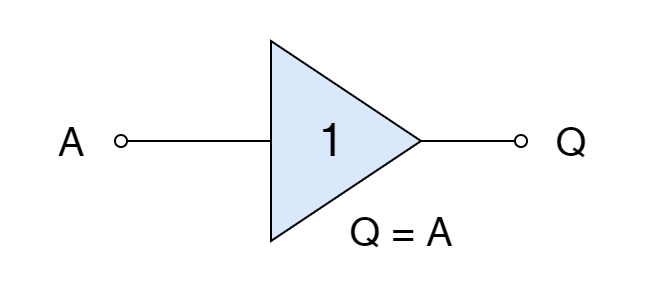
It is a unidirectional device and, as such, allows passage of input towards output i.e. from “A” to “Q”. From the Boolean expression, it is expressed that when input “A” is at logic “HIGH” or “1”, output “Q” is at logic “HIGH” or “1” and, similarly, when input “A” is at logic “LOW” or “0”, output “Q” is at logic “LOW” or “0”. The pattern shown is for a positive logic device such as the 74HC4050 CMOS Hex Buffer Gate.
A Buffer is used to isolate/ separate other devices or circuits from each other in order to prevent affection of functionality or impedance of each other. In addition, a Buffer is used as a driver of high current load, like a transistor, as its fan-out (output drive) capability is very high compared to its input signal. For example, the output port of a microcontroller is set to handle a maximum of 25mA and a buffer is a common solution to isolate sensitive microcontrollers from high-voltage output circuits and/ or to supply a high current. An open-collector Hex Buffer/ Driver can be used for this purpose such as TTL 74LS07 with a 30V output rating. In the following figure, a 74LS07 has been shown with internal circuitry.
Other Buffer Designs
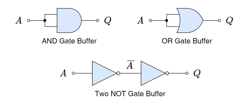
A digital non-inverting buffer can also be constructed using available Basic/ Standard logic gates such as OR, AND, or NOT gates. Simple combinations for accomplishing this non-inverting buffer are shown in the following figure.
Besides the above advantages of a Digital Buffer, there is a major limitation in its functionality as its output will always be connected to its input and that may affect output circuitry. Moreover, it limits flexibility in terms of control and reduction of circuitry. These issues can be solved by using a Tri-state buffer having three (03) different states at its output.
Tri-state Buffer
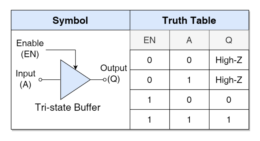
As the name says, it is a type of buffer having three (tri) states of output. These three states of the output of a Tri-state Buffer are achieved by different combinations of inputs and for this, Tri-state, an additional input is used compared to a conventional Digital Buffer. This additional input is a control input enabling the function of a buffer and is termed an “Enable” (EN) input. The usage of this additional input (EN) helps in achieving the third stage of High Impedance (High-Z) which isolates or open the circuit between input & output.
As such, a Tri-state Buffer has three states i.e. “OFF”, “ON”, and “High-Z”. The Control or Enable input can be active at logic “0” or logic “1” and the output of the Tri-state Buffer being non-inverting or inverting which all depends on the IC package. The most commonly used and available Tri-state Buffer ICs are TTL 74LC125 & 74LS126.
Tri-state Buffer Switch Equivalent
In the following diagram, equivalent circuits of Tri-state Buffer in switching modes are shown. The symbol of a Tri-state Buffer is similar to the conventional Digital Buffer but with an additional Control/ Enable (EN) input.
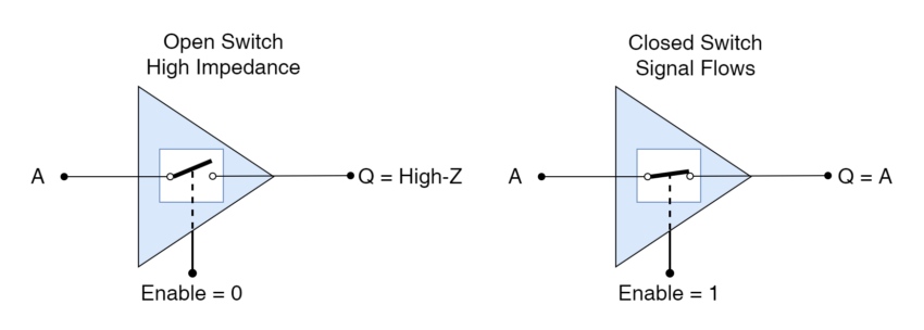
When the “Enable” input is at logic “1” then buffer functionality is enabled and Tri-state Buffer will act as a conventional input. If the “A” input is at logic “0” then the “Q” output will be at “0” as well. Similarly, “Q” goes to logic “1” as “A” input goes to logic “1”.
Whereas, when the “Enable” input is set to logic “0” then the functionality of the buffer is turned off and the output is neither at logic “0” nor logic “1”. The output goes into a High Impedance (High-Z) state which represents an open-circuit condition and isolates/ separates input “A” and output “Q”. Anything present at “A” input is not reflected at “Q” output.
From above, it is observed that Tri-state Buffer has three states: logic “0”, logic “1”, and “High-Z” depending on the “A” and “Enable” inputs. Because of these three states, it is called a Tri-state Buffer. In the third “High-Z” state, it electronically isolates input “A” and output “Q”. Furthermore, at this state, the output is neither at logic “0” nor logic “1”. In a nutshell:
- When “Enable” input is set to “0” or “LOW” state then Buffer’s output becomes open-circuited or goes into High Impedance (High-Z) state.
- When “Enable” input is set to “1” or “High” state then Buffer passes the input signal directly towards the output.
The above functionality is based on a positively enabled (active-high) Tri-state Buffer and is reversed in case of negatively enabled or active-low enable input.
The above functionality of a positively enabled Tri-state Buffer can be represented in a Truth Table form, given below:
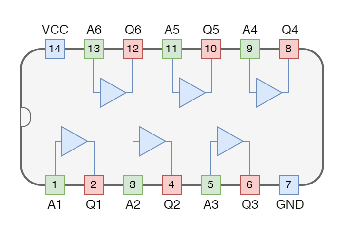
Commercially, Tri-state Buffers are available in IC packages having quad, hex, or octal Tri-state Buffers/ Drivers. In the following figure, TTL 74LS244 Octal Tri-state Buffer with internal circuitry is shown.
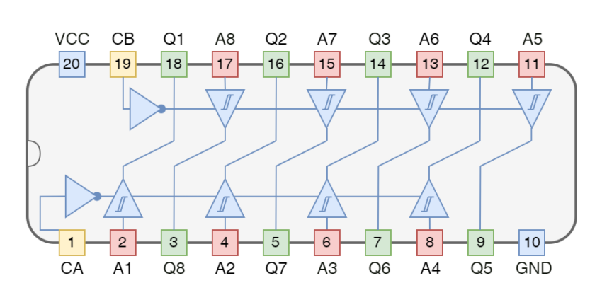
The above octal Tri-state Buffer/ Driver of 74LS244 is divided into two groups of four (04) buffers and each group has its own enable input. In the first group, inputs from A1 to A4 are controlled towards outputs from Q1 to Q4, respectively, using common enable pin “CA”. Whereas, enabling pin “CB” controls the remaining four Tri-state Buffers with inputs (A4 to A5) and outputs (Q5 to Q8).
Single Bus with Multiple Tri-state Buffers
The third state (High-Z) of a Tri-state Buffer aids in connecting multiple devices to a single/ common bus. As this state of high impedance, isolates the input and output which helps in isolating undesired devices from the common bus by disabling relevant Tri-state Buffers and one of them is enabled, at a time, to transfer data towards the bus from the desired device. In the following figure, a decoder has been used to select one of the four devices, at a time, to connect with a common/ shared data or bus.
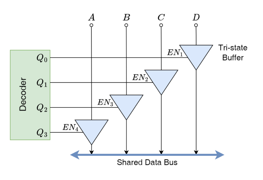
The devices are connected through Tri-state Buffers with a common/ shared data bus or wire, whereas, the control of each Tri-state Buffer is managed using a 2-bit decoder device. The use of a decoder helps in reducing the control wires from four (04) to two (02) only. Furthermore, by using a decoder, only one of the outputs will be set to “1” or “High” avoiding the interruption due to multiple devices communicating at the same time.
Using this decoder, one of the devices will be allowed to communicate with a shared/ common bus by setting the relevant Tri-state Buffer whilst other devices remain isolated due to their disabled Tri-state Buffers. This described combinational logic circuit resembles a 4-to-1 line multiplexer as the four data lines are passed to a single output using select lines. So, using a decoder and Tri-state Buffers, a multiplexer circuit can be constructed.
A Tri-state Buffer can be converted to a conventional Digital Buffer by connecting its “Enable” input to either “Vcc” or “Ground” depending on the type of Tri-state Buffer used. In this way, the Tri-state Buffer will be permanently enabled to pass any signal at input “A” toward output “Q” just like a conventional Digital Buffer.
Bi-directional Buffer Control
A Tri-state Buffer described above enables data to pass through from input “A” to output “Q” only but, not in the reverse direction. In order to enable data passage from both sides, just like a transceiver, two Tri‑state Buffers are placed in inverse parallel along with a NOT gate to invert one of the “Enable” inputs. In the following figure, a Bi-directional Buffer has been shown to demonstrate basic construction and to demonstrate working.
The NOT gate at one of the “Enable” inputs of Tri-state Buffers, ensures that only of them remains enabled at a time. In this configuration, the “Enable” input is working as direction/ data flow control input. For example, when “Enable” is set to “HIGH” then data/ signal flows from “A” to “B” and, otherwise (in case “Enable” is set to “LOW”), from “B” to “A”. So, using “Enable” input, data/ signal can be set to flow in either direction allowing bi-directional communication. The Bi-directional buffers are also commercially available in IC packages such as TTL 74LS245 and CMOS 74ALS620 (inverting) and can be used as Bus Transceivers.
Bus Transceiver
Bus Transceiver is a device based on Tri-state Buffers to allow data/ signal in bi-direction between two buses or to control bi-directional communication between two circuits. The Bus Transceiver is used in bus-oriented systems to facilitate controlled & bi-directional interface/ communication between data buses. In the following figure, an eight (8) line transceiver TTL 74LS245 has been shown.
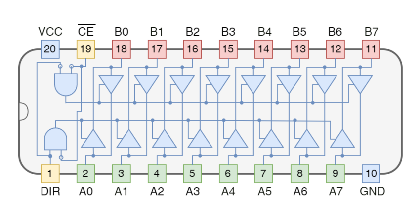
This octal Tri-state Buffer device can be used to interface to an 8-bit data bus for bi-directional & controlled asynchronous data communication. Using “DIR” input, the direction of data flow can be set. For example, when it is set to “HIGH” then data will flow from terminals labeled “A” to terminals labeled “B” and reverses the direction when “DIR” is set to “LOW”. In addition, Chip Enable “CE” input enables or disables the functionality of Tri-state Buffers. The bar on “CE” indicates that it is an inverted logic input and “CE” will be considered enabled when set to “LOW”.
Conclusion
- A Transceiver is a device based on Tri-state Buffers which allows two-way (bi-directional) communication between buses or is used as an interface circuitry.
- A Tri-state Buffer is a form of buffer that allows the passage of signal/ data without any alteration or decision-making.
- A Tri-state Buffer has an additional input of “Enable” and features a third state of High Impedance (High-Z) compared to a conventional Buffer which has only two terminals and two output states.
- A Tri-state Buffer has three (3) output states i.e. “HIGH”, “LOW”, or “High-Z” depending on the signal at data input and state of “Enable” input.
- A Tri-state Buffer in a “Hi-Z” state behaves as an open circuit and isolates both terminals or input & output. This feature makes them suitable for communication with a single/ common/ shared data bus with multiple devices connected.
- A bi-directional/ transceiver can be constructed by placing two Tri-state Buffers in an inverse parallel configuration and using a NOT gate at one of the “Enable” inputs. In this configuration, the “Enable” input acts as a directional control input.
- A Bus Transceiver is based on bi-directional Tri-state Buffers which are used in bus-oriented systems or interface circuitry. An octal Tri-state bi-directional buffer, such as TTL 74LS245, can be used to interface an 8-bit device with a shared/ common data bus.


