Binary Decoder
This essential logic circuit converts n input signals into 2^n outputs. It’s used for memory addressing, chip selection, and translating formats like BCD to decimal.
Binary Decoder
The Binary Decoder is a combinational logic circuit that performs the reverse process of an Encoder. It produces the original binary input data or signals from the Encoded output signals of an Encoder by decoding them. The “Decoder” term defines a device that translates information from one format into another and, more specifically, it transforms “n” binary input signals into an equivalent code using 2n outputs. It is the exact reverse of Encoder which has been discussed in the previous Priority Encoder article.
A Binary Decoder is a digital logic device that may have input binary code of 2-bit, 3-bit, or 4-bit depending on the number of input lines. In general, a decoder can be said to have n-bit code and can represent this n-bit code into an equivalent 2n possible values. The “Binary Decoder” can decode this n-bit code by setting one of 2n outputs to logic “1”. An “Inverter” can be called a 1-to-2 binary decoder as shown below in the figure. When the only input is at logic “0” then the first output is set to logic “1” and for logic “1” input, the second output turns “HIGH”. So, in any case, only one of the outputs is “HIGH” depending on the input data.
A Binary Decoder typically converts a coded signal into another but different coded signal. The coded input signal can either be a Binary or Binary Coded Decimal (BCD) which is converted into a Decimal code using a Binary Decoder. The Binary Decoders have more output lines (2n) compared to input (n) lines and come in the configurations of 2-to-4, 3-to-8, and 4-to-16. Commercially available BCD-to-Decimal decoders include CMOS 4028 and TTL 7442 IC Packages.

In a standardized form, it is an n-to-m decoder and m is less than or equal to 2n. In simple words, the Binary Decoder decides which output line to set “HIGH” by looking at the binary code or number present at the input lines.
2 – to – 4 Binary Decoders
A 2 – to – 4 Binary Decoder, as the name says, has two inputs and four outputs. In the following figure, a 2 – to – 4 Binary Decoder has been shown which comprises an array of four AND gates and two inverters along with its block diagram and truth table. From the truth table, it is obvious that depending on the inputs, one of the outputs will be set to “HIGH”. For example, when both of the inputs are “LOW” then output (Q0) will be set to “HIGH”. Consequently, a “HIGH” state at one of the outputs will indicate the state of inputs or binary code present at the input and can be said to “decode” the input.

In microprocessor memory applications, the Binary Decoders have additional input of “Enable” which can turn ON or OFF the decoding process as per the requirement of memory address selection. The decoders used for such purpose are called “Memory Address Decoders”. An example of a commercially available 2 – to – 4 Binary Decoder is TTL 74155. In larger or complex digital systems, a high order Binary Decoder is required and the number of inputs & outputs can be determined using 2n. So, for three (3) binary inputs, the total outputs are 23 = 8 and present a 3 – to – 8 Binary Decoder.
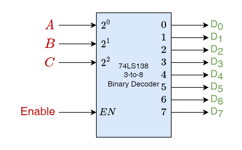
Similarly, four (4) inputs would yield a 4 – to – 16 Binary Decoder (24 = 16). The commercially available 3 – to – 8 and 4 – to – 16 Binary Decoders are TTL 74138 and TTL 74154, respectively. The Binary Decoders can have equal or less than binary outputs given by 2n. For example, a BCD (Binary Coded Decimal) to 7-segment converter has four (4) inputs and only seven (7) outputs out of a total of 24 = 16 outputs. A BCD to 7-segment Decoder is commercially available as TTL 7447 package.
4 – to – 16 Binary Decoders
A 3 – to – 8 Binary Decoder shown above is used to implement 4 – to – 8 variants with the help of an additional input “Enable”. This configuration of the 4 – to – 16 Binary Decoder is shown in the following figure.
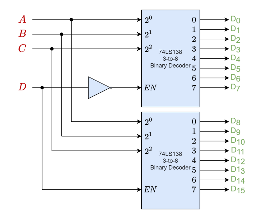
Each 3 – to – 8 Binary Decoder works the way described above except the fourth input (D) enables either of the two 3 – to – 8 Binary Decoders. Hence constituting a 4 – to – 16 Binary Decoder. Such a configuration relates to the number of inputs (AND gates) a decoder can accommodate without fan-out of gates driving them to become large. The Binary Decoders are usually constructed using AND plus NOT gates or just NAND gates. The AND gate configuration of a Binary Decoder produces a “HIGH” output when one of the inputs is “HIGH”. On the other hand, the NAND configuration yields “LOW” at the respective output when one of the inputs is “HIGH”. The NAND gate configuration is cheaper to produce as it requires fewer transistors to implement.
2 – to – 4 Line NAND Binary Decoder
As discussed above that a Binary Decoder based on AND gates gives logic “HIGH” on one of its outputs whereas the NAND gates base Binary Decoder gives logic “LOW” on one of its outputs whilst all other outputs are set to “HIGH” logic state. In the following figure, a 2 – to – 4 Binary Decoder using NAND gates is shown.
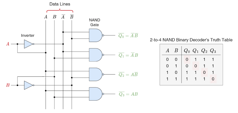
In addition to two binary inputs, a third input “Enable” is used to “OFF” and “ON” the function of decoding by setting it to “LOW” and “HIGH” states, respectively. In NAND gate configuration, Enable = 0 sets the outputs to logic “LOW” or “0” irrespective of the states of inputs.
Memory Address Decoder
The most important application of the Binary Decoder is found in memory systems where a particular memory address is selected or decoded. This application is more profound in larger or complex memory systems where a number of memory chips are connected to a microprocessor through a single data bus. The memory chips are selected individually one at a time using the Address Decoding technique. The specific address of a memory chip is represented by coded data input and the outputs select the particular memory chip related to that address. The memory chips or storage devices have “Chip Select” or “CS” which invokes them when set to “HIGH”. The outputs of the Memory Decoder are connected to the “CS” inputs of all the memory chips.
The coded input or memory address selects or de-selects a relative memory chip through a particular output line connected to the “CS” pin of that specific memory chip. Generally, at an output line, a logic “HIGH” selects and a logic “LOW” de-selects a particular memory chip. Using this memory decoding technique, a 2 – to – 4 memory decoder can be used to select four (4) memory chips using only two (2) binary inputs.
Example of a Memory Address Decoding
Considering each memory location contains a byte (8-bits) of data and there are a total of 128 such locations. This constitutes a single memory chip having (128 X 8) = 1024 bits or 1 Kb of storage capacity. This single memory chip requires an eight (8) bit data bus for reading 8 bits (1 byte) from each memory location and a seven (7) bit address line to represent from 0 to 127 (27 = 128) memory addresses. Now, by using 3 – to – 8 memory decoders, the memory capacity can be increased to 8 X 1 kb = 8 Kb and a stack of eight (8) such memory chips can be managed. A particular memory chip is selected using a “CS” pin which is driven through a 3 – to – 8 Memory Decoder and then a 7-bit address line selects a specific memory address amongst 128 addresses of that particular memory chip. This is illustrated using the following figure.
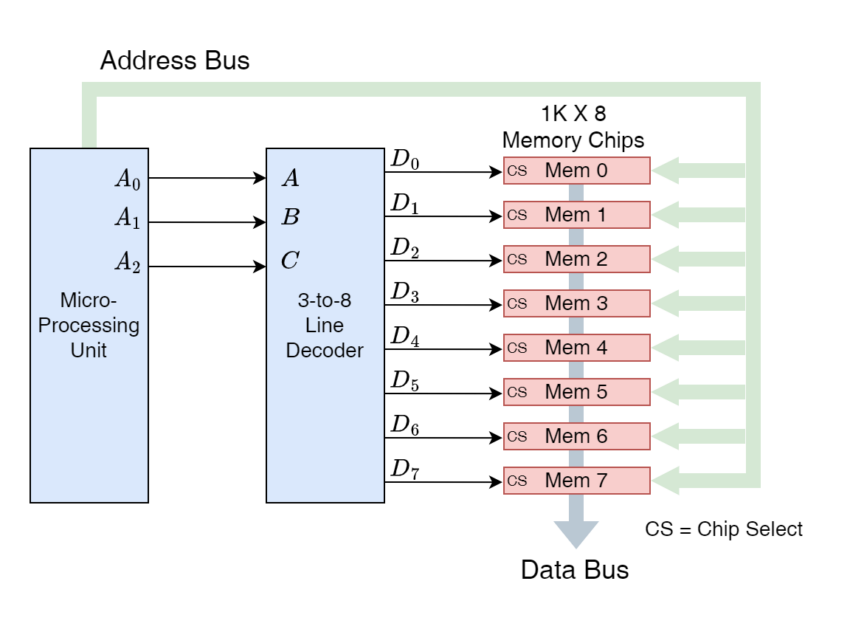
In the above figure, a Microprocessor Unit (MPU) generates a 10-bit memory address which constitutes of two parts i.e. lower and upper. The lower part comprises three (3) bits to select a particular memory chip whereas the upper part consists of seven (7) bits that select a specific memory location out of 128 locations. The lower part (3 bits) is coded input to a 3 – to – 8 memory decoder which selects the particular memory chip of 1 Kb.
For example, if MPU issues an address of “0110000101” then the lower part (3 LSB bits) i.e. “101” select the 5th memory chip, and the upper part i.e. “0110000” points to the 49th memory location as the memory location starts from 0 so 48th position means a 49th Memory location.
Conclusion
- A Binary Decoder is a combinational logic circuit that decodes the n-bit binary coded data into 2n binary outputs. It performs the reverse process of a Binary Encoder.
- Binary Decoders have input and output configurations of 2 – to – 4, 3 – to – 8, 4 – to – 16, and so on. For an n-bit Binary Input, a Binary Decoder has 2n binary outputs.
- Binary Decoders are constructed using AND or NAND logic gates. The AND constitution outputs a “HIGH” logic at the selected output, whereas, a “LOW” logic in the case of the NAND structure. The NAND composition is cheaper to construct as it uses fewer transistors.
- The Binary Decoders are significantly used in Memory Address Decoding of a complex/ larger digital system. Using the Binary Decoder, a number of memory chips are connected to a single data bus one at a time using the “Chip Select” input pin.
- The Binary Decoders are commercially found in 2 – to – 4 (TTL 74154), 3 – to – 8 (TTL 74138), and 4 – to – 16 (TTL 74155) IC Packages.


