The Zener Diode
The Zener Diode A diode is the simplest form of a semiconductor device in which P-type and N-type semiconductors are fused together to form a PN junction. Around this PN junction, a depletion layer is formed having opposite ions.
The Zener Diode
A diode is the simplest form of a semiconductor device in which P-type and N-type semiconductors are fused together to form a PN junction. Around this PN junction, a depletion layer is formed having opposite ions. The Zener diode is a type of diode and the basic difference between a simple diode and a Zener diode is the level of doping in semiconductor materials. The doping level of semiconductor material is controlled during the manufacturing process. The Zener diodes have a high level of doping which also contributes to their specifications to operate at different levels of voltages. Due to this high level of doping, the depletion layer of PN-junction is thin compared to the PN junction of a simple diode. This gives special characteristics to the Zener diode to operate in the reverse direction.
Forward-biased Characteristics
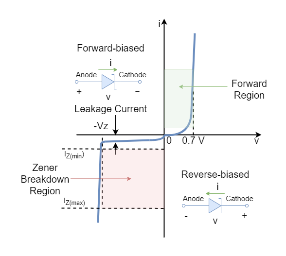
The forward characteristic of the Zener diode is similar to the simple diode and the forward current is an exponential function of forwarding voltage drop. A little variation in voltage drop causes a rapid rise in current. Normally, a voltage drop of 0.7 Volts across the PN-junction is sufficient to make the Zener diode forward-biased. A forward-biased Zener diode is shown below:
Reverse-biased Characteristics
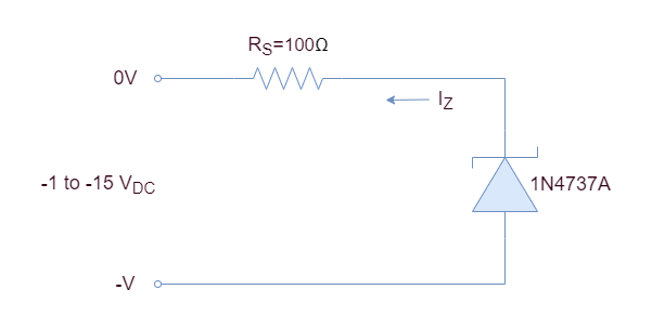
The diode when operated in reverse-biasing mode, no current flows through it until an avalanche breakdown occurs upon reaching a certain reverse voltage. Under this condition, a large stream of electrons could damage a signal diode. However, in the Zener diode, a Zener breakdown occurs due to the strong electric field produced by a thin depletion layer of the PN junction. The voltage at which Zener breakdown occurs is called VZ (Zener Voltage). The Zener diodes are produced to have different levels of Zener voltages as per application and voltage requirements. Once Zener breakdown occurs, a further increase in reverse voltage does not cause any further voltage drop and remains constant up to a certain voltage level until an avalanche breakdown occurs. In a nutshell for a reverse-biased Zener diode, it remains off (minor amount of current flows) from 0V to Zener Voltage (VZ). From VZ to avalanche breakdown, small changes in applied voltage cause a rapid increase in reverse current flow.
The characteristics of a typical Zener diode is shown in the following figure:
Specifications
Similar to other electronic components Zener diodes have rating/ specifications at which they can be operated such as Nominal Voltage, Maximum Reverse Voltage, Power Dissipation, Power Rating, and Packaging, etc. Normally used specifications are:
- Zener Voltage (VZ): Reverse breakdown voltage (Normal Range: From 2V to 1000V).
- Zener Current (IZ): Maximum rate amount of current at Zener Voltage (Normal Range: From 200uA to 200A).
- Rated Power: Maximum amount of power that a Zener diode can dissipate. It is a simple multiplication of Zener Voltage (VZ) and maximum Zener Current (IZ).
- Voltage Tolerance: Normally ±5%.
- Zener Resistance (RZ): Resistance exhibited by Zener diode.
- Package: THT, SMD, and PDIP (integrated Circuits).
Applications of Zener Diode
The Zener diode has a large number of applications in electronic circuits and some of them are listed below:
Voltage Regulator:
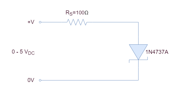
The most common use of a Zener diode is in power supplies as a voltage regulator. At Zener Breakdown and beyond in reverse direction, the voltage drop i.e. Zener Voltage (VZ) remains constant and any variation in applied voltage does not cause any change in it. A reverse-biased Zener diode in series with a current limiting resistor supplies a constant voltage to loads connected parallel to it. The load voltage remains equal to Zener Voltage (VZ).
Example
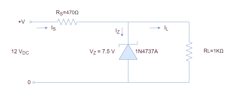
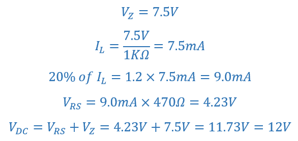
For the circuit given in figure-5 at least, a VDC of 12V is required to produce an output of 7.5V with a load of 1KΩ.
A more improved voltage regulation circuit can be designed with the help of an operational amplifier which is shown below in figure 6:
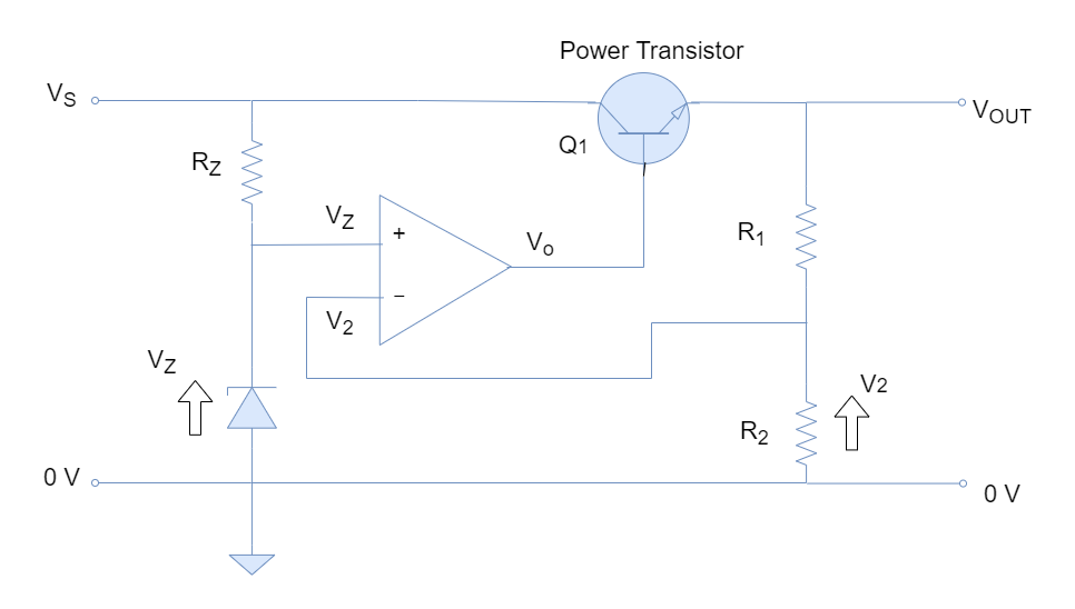
The Zener diode is placed at the non-inverting input of the op-amp setting Zener voltage as a reference voltage (V1). The other input i.e. inverting (V2) is taken from the output voltage. The V2 voltage is dependent on the output voltage (Vout) and any change in output voltage is reflected back in V2. The increase in load leads to a drop in output voltage which drops the input voltage (V2). The Op-amp tries to keep both inputs i.e. V1=VZ & V2 equal and to attain this condition Op-amp’s output voltage (Vo) increases which leads to compensate for the drop in load voltage. Similarly, whenever there is a decrease in load condition then an increase in V2 leads Op-amp to decrease its output voltage (VO). This decreased transistor (Q1) base current and, hence, the output voltage decreases.
The equation for the output voltage of this circuit is given by:
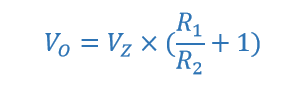
For example to obtain an output voltage of 10V:
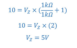
A Zener diode with a Zener voltage of 5V is required.
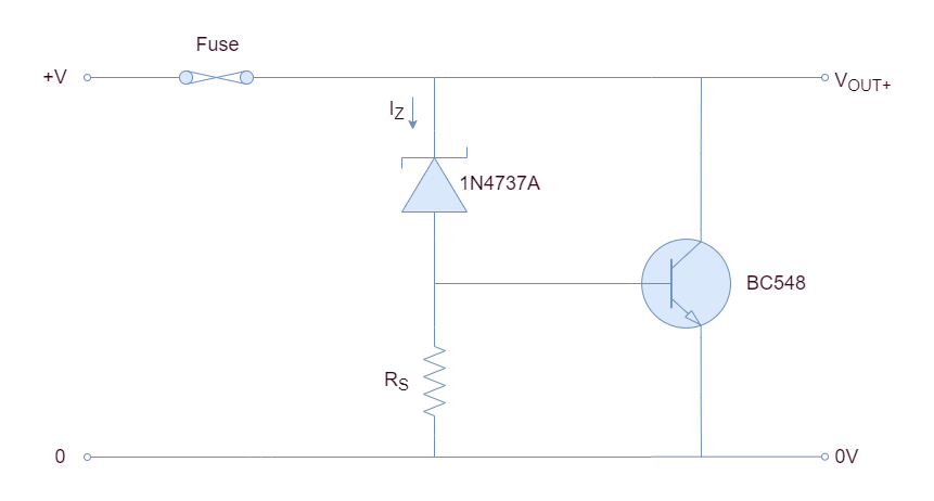
Overvoltage Protection
For the circuit shown in the figure-7, any voltage above Zener Breakdown causes a current flow through the resistor. A voltage drop occurs across this resistor which turns on the transistor and shorting the path. The heavy current flows and opens the fuse to disconnect the circuit.
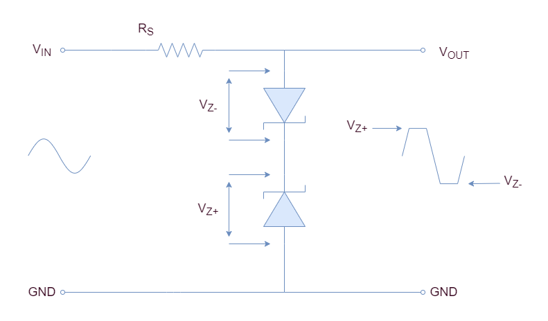
Clipping Circuits
When AC voltage is applied to the Zener diode then any voltage above Zener breakdown is clipped off. The two diodes connected in series with opposite directions cause clipping of AC in both positive and negative cycles. An example of a clipping circuit is a sine to square wave converter.
Conclusion
- Zener diode behaves as a simple diode (on) when forward-biased.
- Zener diode can acts as a switch (off) when reverse-biased up to Zener Voltage (VZ).
- From Zener Voltage (VZ) to Avalanche Breakdown, the output of Zener diode remains pretty constant equaling Zener Voltage (VZ).
- When operating in Zener mode, a small change in input voltage causes a rapid increase in Zener Current (IZ) which can be limited by using a series resistor (RS).
- Zener diodes are used most commonly in power supplies, voltage regulators, protection circuits, and waveshapers.
- Before using a Zener diode, it is always recommended to consult its datasheet to know its rated parameters as per design requirements.


