Semiconductor Theory
Semiconductor Theory As it is obvious from the name, semiconductors are those materials having conductivity in between conductors and insulators. Conductors are those materials that impose minimum resistance in the flow of electrons or current.
Semiconductor Theory
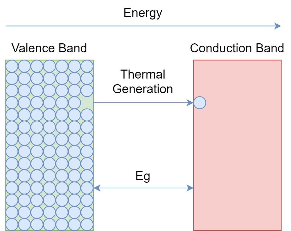
As it is obvious from the name, semiconductors are those materials having conductivity in between conductors and insulators. Conductors are those materials that impose minimum resistance in the flow of electrons or current. Whereas, insulator materials impose high resistivity and, thus, no current flows in them. As we know, for an atom, there are valence electrons, and when they gain a sufficient amount of energy they jump into the conduction band. The forbidden band is there in between these valence and conduction bands. The flow of current is due to the presence of free electrons in the conduction band.
In conductors, the valence band and conduction band overlap with each other, and electrons require a minimum amount of energy to jump into the conduction band. The good conductors are Copper, Silver, and Aluminum. Insulators have wider forbidden energy gaps and electrons require a significant amount of energy to shift into the conduction band. Therefore, insulators have poor conductivity as there are no electrons in the conduction band. The good insulators are glass, porcelain, rubber, and ceramics.
The forbidden energy gap in semiconductors is not that wide, as in insulators, nor it is overlapping, as in conductors. It is somewhere, in between, and at room temperature valence electrons of the semiconductor get enough energy to jump into the conduction band. However, the number of electrons jumping into the conduction band is not that much to cause a good current flow. Examples of semiconductors are Silicon, Germanium, and Germanium Arsenide.
Semiconductors are of two kinds: single-element, such as Silicon and Germanium; and compound semiconductors, such Gallium-Arsenide. The compound semiconductors are used in some special electronic applications such as in devices involving light e.g. LEDs diodes.
Intrinsic Semiconductors
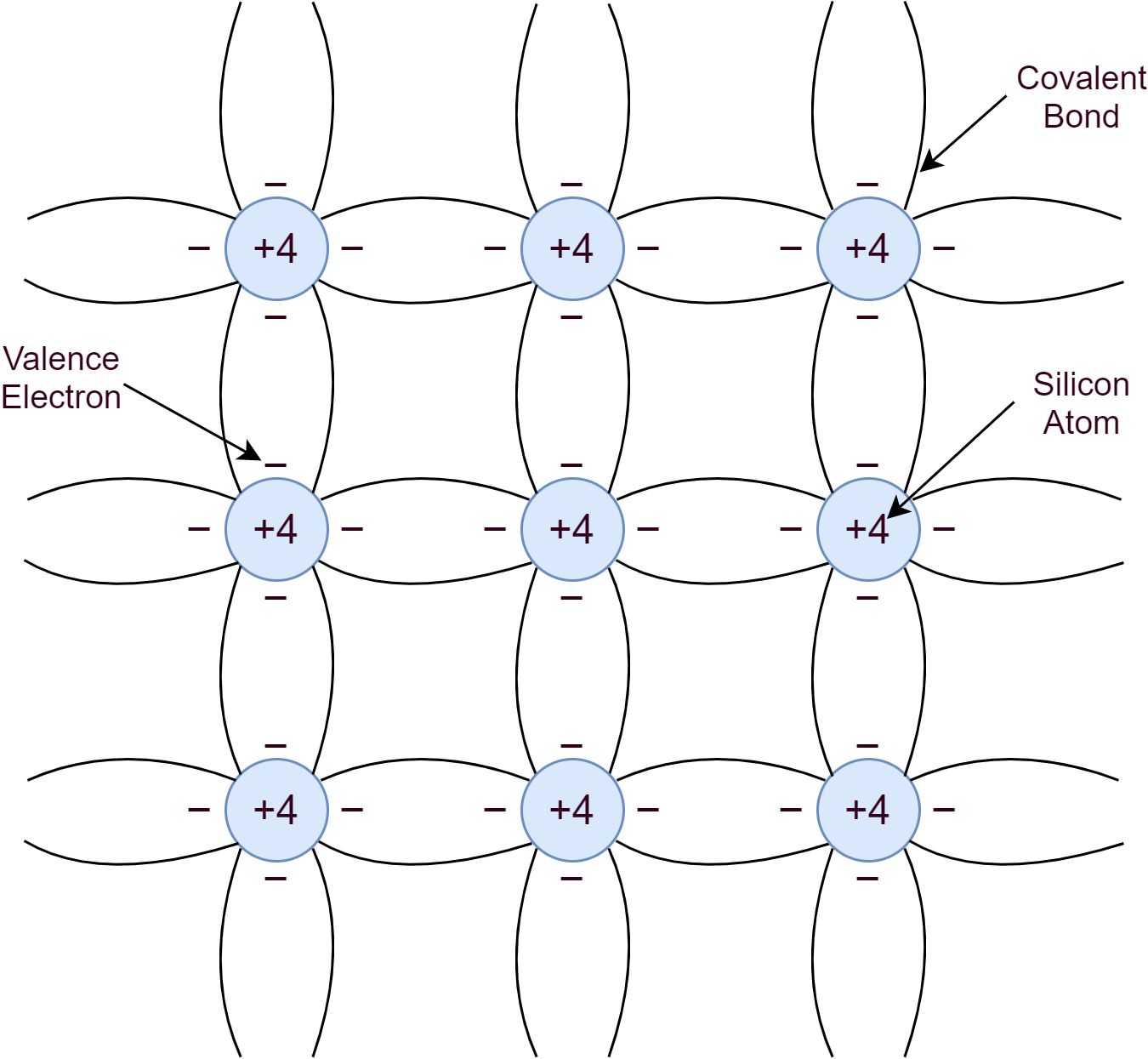
An intrinsic semiconductor is a pure form of a semiconductor material such as Silicon or Germanium. Silicon belongs to Group-IV of the periodic table and as such has four valence electrons. These four valence electrons form covalent bonds with the valence electrons of neighboring atoms. This makes a pure crystal of regular lattice structure.
At low temperatures, near to absolute zero (0K), the covalent bonds remain strong enough to make Silicon act as an insulator. However, due to thermal generation, energy is sufficient enough to break some of the covalent bonds at room temperature and create free electrons. Silicon crystal structure when subjected to an electric field or potential, makes free electrons to conduct electricity. The freed electron leaves behind a vacancy/ hole or a positive charge. An electron may fill up this hole from the neighboring atom and the process may keep repeating. In other words, moving a hole or positive charge to conduct electric current. The process of filling up a hole with an electron is recombination.
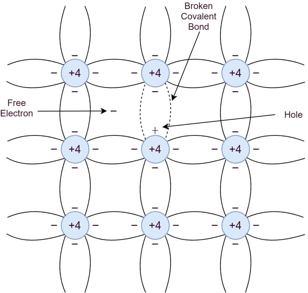
An increase in temperature causes dislodging of more covalent bonds and, thus, generating more free electron-hole pairs, eventually, increasing the conductivity of Silicon crystal. The number of electrons and holes generated are equal in numbers and results in equal concentrations per unit of volume. The thermal generation rate of electron-hole pairs is equal to the recombination rate at thermal equilibrium. So, the concentration of electrons is equal to the concentration of holes per unit volume.
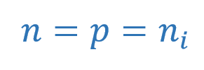
Where “ni“, is the number of electrons and holes per unit of volume (cm3) at a certain temperature for intrinsic material. It is determined by:
![]()
Where, for Silicon
![]()
![]()
Boltzmann’s constant,
![]()
“T” is the temperature in Kelvin, “Eg” is bandgap energy (to free an electron) and “eV” is electron-volt.
![]()
Extrinsic Semiconductor
An intrinsic semiconductor has an equal concentration of electrons and holes created by thermal generation and this concentration is quite low to cause a flow of current. Moreover, this concentration is dependent on temperature and, at room temperature, can cause abrupt changes in the concentration of charge carriers. The combination of an intrinsic semiconductor with another material (impurity) in a precisely controlled manner, can eliminate these issues. This process is doping and the material formed by doping is an extrinsic semiconductor.
This doping process introduces impurity atoms in the Silicon crystal in order to increase the number of charge carriers either negative (electrons) or positive (holes) in a precise manner such that the Silicon crystal structure remains intact in the original shape/ structure. In order to increase the concentration of electrons, the Silicon is doped with atoms having one surplus electron i.e. the elements of Group-V of the periodic table. The most commonly used doping element to increase the concentration of electrons is Phosphorous. Whereas, to increase the concentration of holes, Silicon is doped with elements having one less electron. For example, Boron which belongs to Group-III of the periodic table.
N-type Semiconductor
When the intrinsic Silicon is doped with an element, having five (5) valence electrons, the concentration of negative (n) charge carriers increases, and, as such, the semiconductor is called N-type. In the careful process of N-type doping, the Phosphorous shares four of its electrons with neighboring atoms of Silicon to form covalent bonds. Whilst, leaving behind a free electron and, in this way, each Phosphorous atom donates a free electron to the Silicon crystal. In N-type doping, Phosphorous is a donor element (donating electrons) and no holes are there. The majority of carriers are electrons.
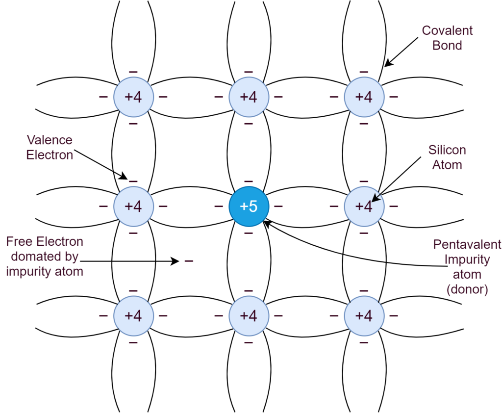
The concentration of donor atoms is much greater than the concentration of thermally generated charge carriers. The major concentration of negative (N) charge carrier is due to doping and is independent of temperature. Whereas, the sole concentration of holes is due to thermal generation and can be calculated by the formula given above.
In the N-type semiconductor, the concentration of electrons (negative charge) is much higher and independent of temperature. So, electrons are majority carriers and holes are minority carriers in N-type semiconductor.
P-type Semiconductor
When the intrinsic semiconductor, such as Silicon, is doped with elements having three (3) valence electrons under a precisely controlled environment. The trivalent impurity atoms make four (4) covalent bonds by accepting electrons from the neighboring Silicon atoms. The Silicon atom donates electrons, here, and leaves behind a hole/ positive charge. The semiconductor, where Silicon atoms donate electrons to impurity and create positive ions, is P-type semiconductor. Now, holes/ positive charges are the majority carriers.
In a P-type semiconductor, the intrinsic semiconductor is doped with elements of Group-III e.g. Boron. The three (3) electrons of this trivalent Boron makes four (4) covalent bonds by accepting an electron from Silicon, as depicted in the following figure:
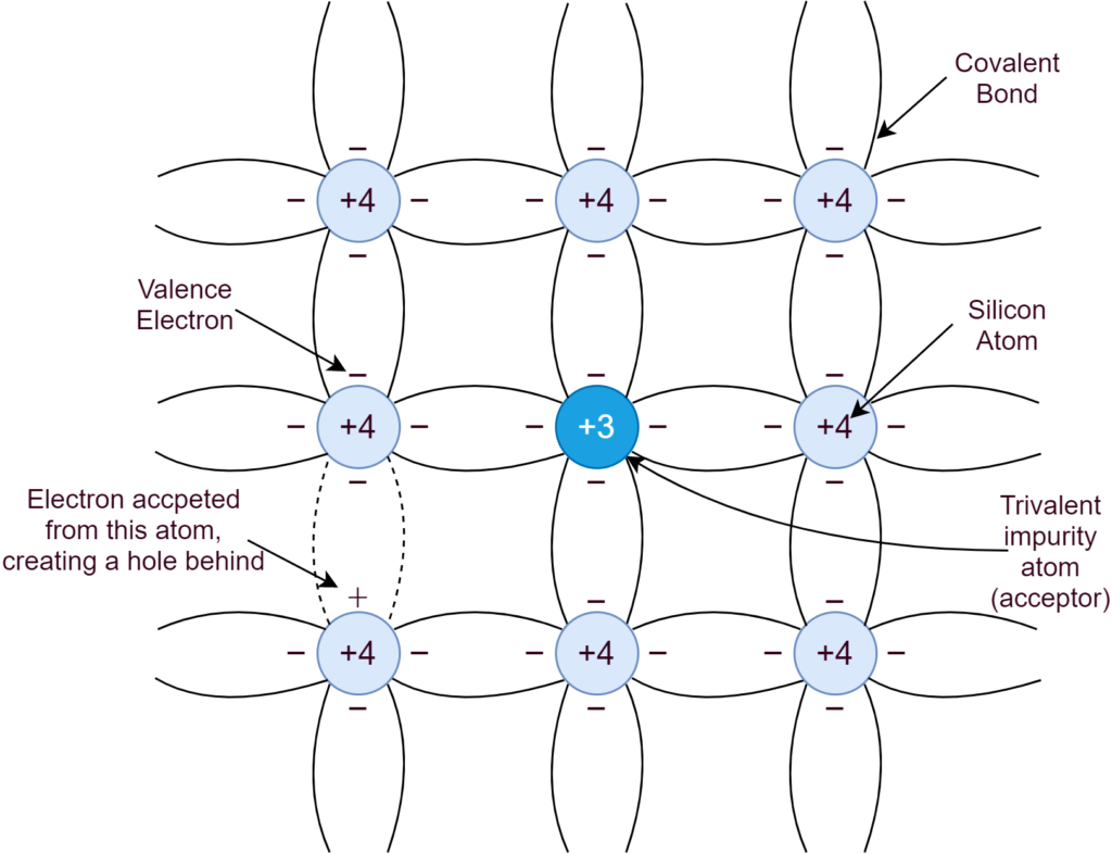
The hole generated by adding impurity, attracts electrons from neighboring Silicon atoms and, effectively, makes a hole(s) shifting from one place to another and this process keeps repeating. Due to high impurity concentration, the holes are significantly high in numbers as compared to electron-hole pairs, generated due to thermal generation. This P-type doping makes holes/ positive charges as the majority carriers and electrons as the minority carriers. The majority carrier’s concentration is dependent on doping level and, whereas, the minority carrier is dependent on thermal generation.
It is eminent to mention here that a pure semiconductor material is neutral. In N-type semiconductors, the majority carriers (electrons) neutralize the bound positive charges of Phosphorus atoms. Similarly, in P-type semiconductor, the majority carriers (holes) neutralize the negative bound charges of Boron atoms.
Electric potential, when applied, causes the current flow in the semiconductor. In semiconductor two types of current flows: drift current that is due to drift of charge carriers; and diffusion current that is due to diffusion of charge carriers into less concentrated areas.
Conclusion
- Intrinsic semiconductors have mobility carriers due to thermal generation only and they are minority carriers in doped semiconductors.
- An impurity added to an intrinsic semiconductor makes it a doped semiconductor.
- In doped semiconductors, the majority carriers are either electrons (N-type) or holes (P-type) and their concentrations are dependent on doping level.
- Doping of intrinsic semiconductors with pentavalent impurity atoms makes electrons as majority carriers. A property of N-type semiconductor.
- In N-type semiconductor, impurity is the donor of electrons and has a bound positive charge.
- Doping of intrinsic semiconductors with trivalent impurity atoms makes holes as majority carriers. A property of P-type semiconductor.
- In P-type semiconductor, impurity is the acceptor of an electron and has a bound negative charge.
- Both N-type and P-type semiconductors are electrically neutral, as a whole.


