PN Junction Theory
PN Junction Introduction It is better to briefly revise the basic semiconductor theory before starting the PN junction theory. As we know, the N-type semiconductor has electrons as majority carrier and holes as minority carrier.
PN Junction Introduction
It is better to briefly revise the basic semiconductor theory before starting the PN junction theory. As we know, the N-type semiconductor has electrons as majority carrier and holes as minority carrier. The impurity in N-type semiconductor is a donor and has a bound positive charge which neutralizes majority electrons as a whole. In the same way, the P-type semiconductor has holes as a majority carrier and electrons as a minority carrier. The impurity in P-type semiconductor is acceptor and has a bound negative charge which neutralizes majority holes.
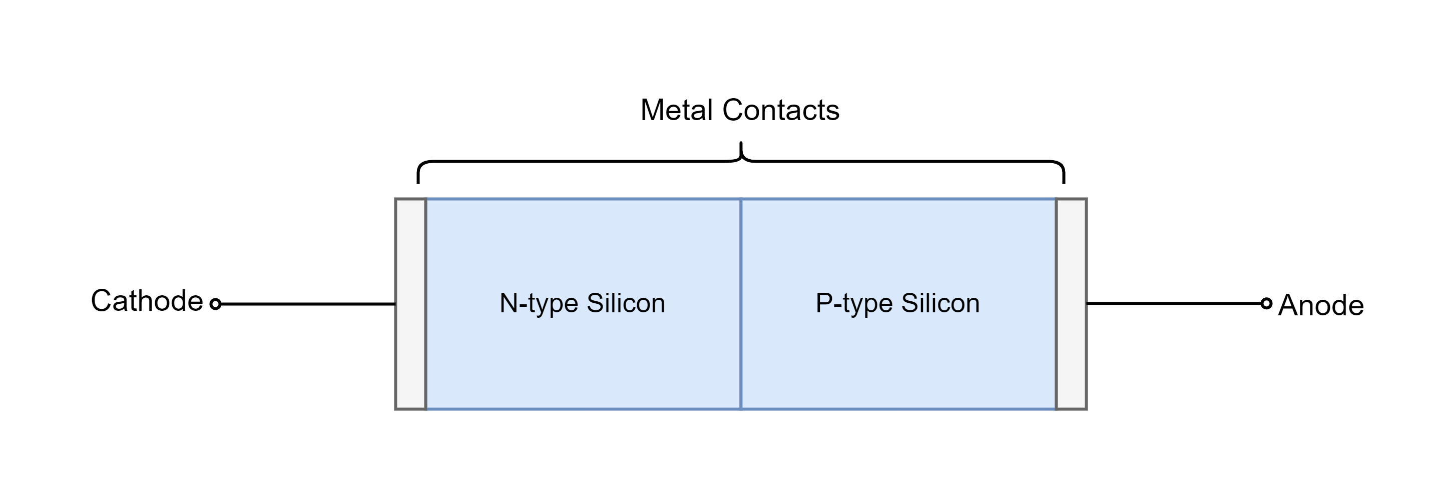
In the following figure, a physical structure of the PN junction is shown. Both P-type and N-type semiconductors are in contact with each other. Actually, both regions are made of the same silicon crystal structure/ part and this, silicon crystal, is further doped to form P-type and N-type regions. These regions are further connected to external wires through aluminum contacts. The terminals are named “anode” and “cathode” as per diode naming terminology.
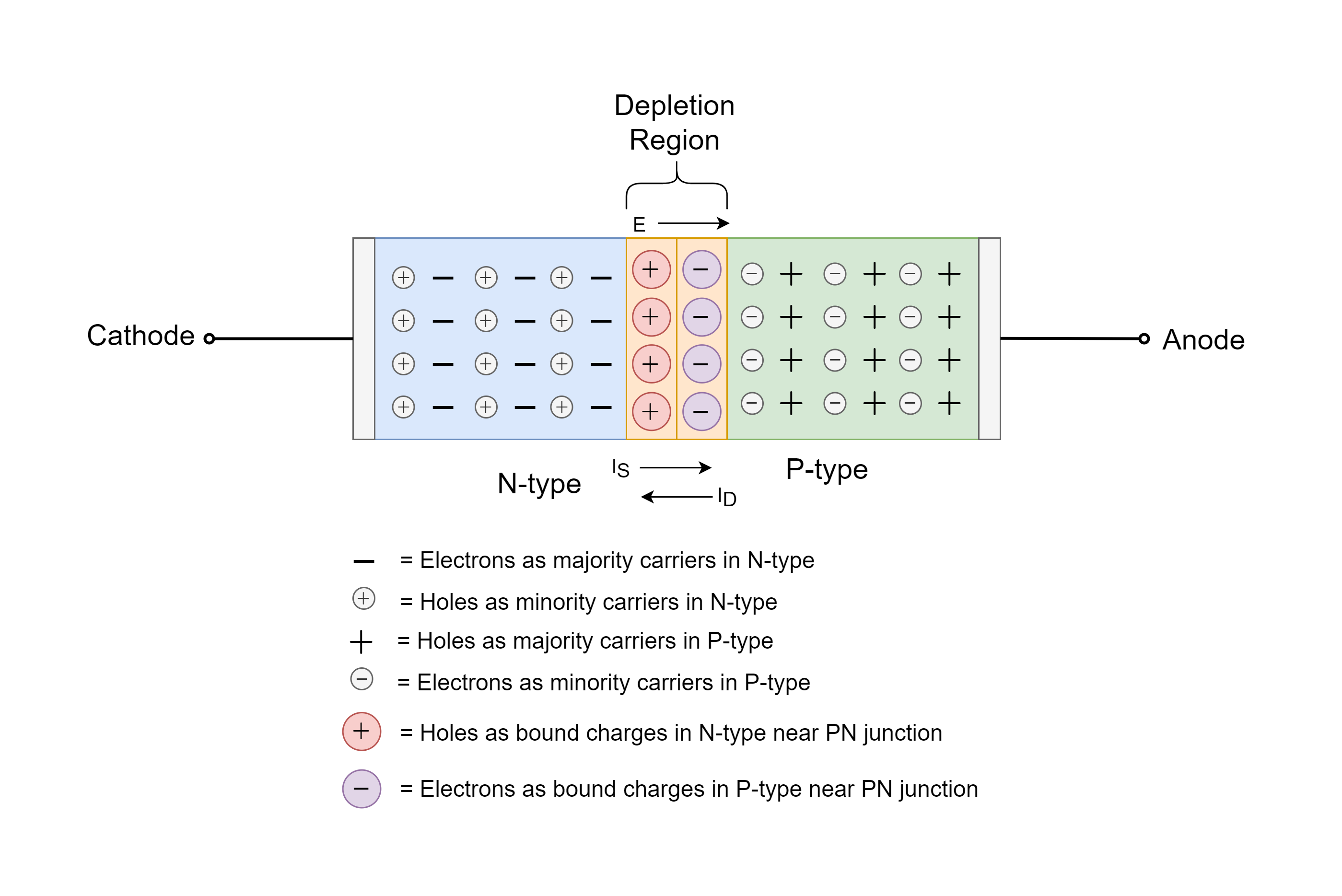
In the following figure, a PN junction is shown under the open-circuit condition which means terminals are not connected to an external voltage. Here, in the P-type region, plus “+” sign indicates holes as the majority carriers, and the circled negative “-” sign indicates the bound charge of impurity. In the N-type region, the negative “-“ sign indicates electrons which are the majority carriers, and the circled plus “+” sign indicates the bound positive charge of impurity. In the figure, thermally generated minority carriers i.e. holes and electrons in N-type and P-type regions respectively, are not shown.
The Diffusion Current (ID)
When the silicon crystal is doped into P-type and N-type regions then some of the majority holes and electrons diffuse in other regions due to concentration difference. The concentration of holes is high in the P-type region compared to the concentration of holes in the N-type. Similarly, the concentration of electrons is high in the N-type region compared to the concentration of electrons in the P-type. Due to this, some of the majority of electrons diffuse into P-type regions, and, similarly, some of the majority holes diffuse into the N-type region. These both diffusions constitute a diffusion current (ID) from the P-type to N-type region.
The Depletion Region
Some of the majority electrons diffusing across the PN junction to P-type region, recombine with some of the majority holes. Due to this recombination process, some of the holes disappear in the P-type region and uncover the negative bound charges of impurity. This disappearance of holes in P-type, near the PN junction, causes depletion of positive charges, and as such negative charge appears.
The majority of holes diffusing into the N-type region recombine with some of the majority electrons of the N-type and make them disappear as well. This disappearance of electrons in N-type, near the PN junction, depletes the region from electrons. This depletion uncovers the bound positive charges of impurity atoms and positive charges appear in the N-type region close to the PN- junction.
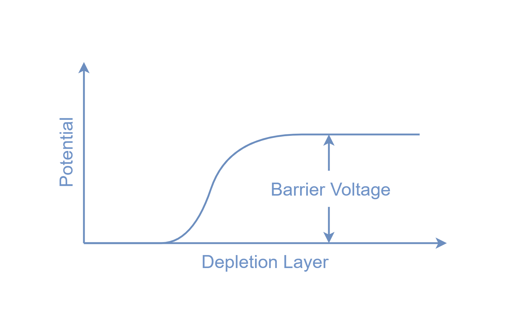
So, there is a carrier-depletion region on each side of the PN junction, the P-type will be negatively charged and the N-type will be positively charged. The formation of charges causes an electric field (E) across the depletion and a voltage appears to have N-type as positive voltage relative to P-type having negative voltage. This electric field, actually, opposes the diffusion of majority carriers into other regions and the voltage developed, due to this field, acts as a barrier. The voltage barrier has to be overcome to diffuse majority carriers into other regions. The larger the barrier voltage, the smaller the number of carriers that will be able to diffuse to constitute the diffusion current. Thus, the magnitude of diffusion current (ID) depends on the barrier voltage.
The Drift Current (IS)
Besides, diffusion of majority carriers into other regions there is the diffusion of minority carriers into other regions as well. These minority carriers are due to thermal generation and their concentration depends on temperature. The minority holes in the N-type region, near the PN junction, experiences the electric field and diffuse into the P-type region. Similarly, the minority electrons of P-type are swept into the N-type region due to the electric field. This flow of holes from N-type to P-type and of electrons from P-type to N-type constitutes a drift current (IS). The direction of this drift current (IS) is from N-type to P-type. As the concentration of minority carriers is dependent on temperature, the drift current (IS) magnitude changes with the temperature and is independent of barrier voltage.
Equilibrium (ID = IS)
When this PN junction is not connected to an external voltage then under this open-circuit condition:
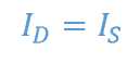
The diffusion current due to the depletion layer will be equal to the drift current due to thermal generation. This means that hole currents will be equal i.e. due to diffusion and drift of holes. On the other hand, electron currents will be equal i.e. due to diffusion and drift of electrons. This equilibrium condition is maintained by the depletion voltage. For example, if there is an increase in ID then the more majority carriers will diffuse into other regions which will uncover more bound charges, ultimately, widening the depletion layer. The barrier voltage will increase due to PN junction widening which will reduce ID until an equilibrium is achieved.
Junction Voltage
Under the open-terminal condition, the voltage across the depletion layer or the barrier voltage will be:
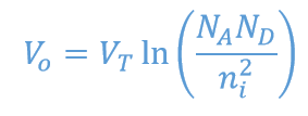
The above equation shows that the barrier voltage is dependent on the doping concentrations as well as on the temperature. It is worth mentioning here that for silicon, the PN-junction voltage barrier is between 0.6 V to 0.9 V, at room temperature.
Conclusion
- When P-type and N-type silicon regions are combined then the majority carriers of each region diffuse into other regions.
- Electrons of the N-type region diffuse into the P-type and holes from the P-type diffuse into the N-type region.
- Diffusion of these majority carriers into other regions constitutes a diffusion current (ID).
- The majority carriers diffusing into other regions recombine with opposite majority charges and make them disappear. Which uncovers the bound charges.
- Electrons diffusing from N-type to P-type recombine with holes (which make holes disappear) uncovering bound negative charges of impurity atoms.
- Holes diffusing from P-type to N-type recombine with electrons (which make electrons disappear) uncovering bound positive charges of impurity atoms.
- Adjacent to the PN junction, positive charges appear in N-type and negative charges in P-type regions.
- The appearance of these bound charges establishes an electric field (E) and barrier voltage (VO).
- Barrier voltage (VO) opposes diffusion of majority charges only.
- Thermally generated minority carriers diffuse into other regions as well but in opposite direction to the majority carriers, giving rise to drift current (IS).
- In equilibrium (open-terminal condition)
- ID = IS
- The magnitude of drift current (IS) depends on temperature.
- In equilibrium (open-terminal condition)
- In open-terminal condition, barrier voltage establishes equilibrium by either increasing or decreasing the diffusion current (ID).


