Schottky Diode
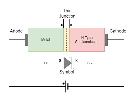
Schottky Diode The Schottky diode is a semiconductor diode formed by the junction of metal with the semiconductor material. It is named after the German physicist W.
Schottky Diode
The Schottky diode is a semiconductor diode formed by the junction of metal with the semiconductor material. It is named after the German physicist W. H. Schottky. The Schottky diode is also known as a hot-carrier diode and Schottky barrier diode. It has a low forward voltage drop and high switching speed. It is used in a variety of switching, rectification, and wave-shaping circuits. They are mostly used in digital logic circuits and solar panels. The transistor-transistor logic (TTL) uses these Schottky diodes in 74S, 74LS, 74AS & 74ALS bipolar logic series.
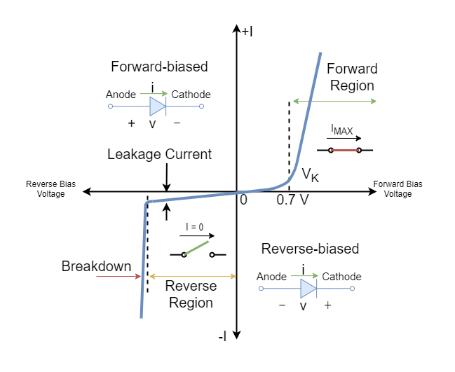
The conventional diode comprises of PN junction which is formed by combining P-type and N-type semiconductors. It consists of both majority carriers and minority carriers in both P-type and N-type semiconductor materials. The forward biasing of conventional diode faces low resistance of PN junction and current flows through it. The typical forward voltage drop of a Silicon diode ranges from 0.7 to 0.9 V. In reverse biasing, the PN junction diode offers high resistance and a small leakage current flows through it. This characteristic is especially useful in rectification and switching applications. The characteristic of the PN junction diode is non-linear because the DC resistance offered by the junction changes with the voltage and current applied to it in forward and reverse-biasing conditions.
The IV-Characteristic of a conventional diode is shown below. The diode starts conducting when the external biasing voltage applied exceeds the knee voltage (VK) in forward biasing. The silicon diodes have knee voltages in the range of 0.6 to 0.9 Volts, whereas, Germanium diodes have knee voltages around 0.3 volts. From IV-Characteristic it is clear that conventional diode offers resistance to a greater extent in reverse biasing and a negligible amount of leakage current flows until breakdown occurs.
Whereas, the Schottky diodes offer less forward voltage drop and fast switching action as compared to conventional diodes. These Schottky diodes can be used in a variety of applications similar to that of conventional diodes especially in solar panels, and digital logic circuits, etc. The Schottky diodes are formed by bonding the metal electrode with the N-type semiconductor instead of the P-type semiconductor. Due to this bonding of a compound metal with the N-type material, there exists no depletion layer which classes them as a unipolar device.
Construction and Working Principle
The semiconductor used in N-type material of Schottky diode is lightly doped and a highly conductive material compound is used to bond with it. The metal compound used is Silicide which is a highly conductive metal compound. The absence of depletion layer and low metal resistance give characteristics of very low forward voltage drop to the Schottky diode. The forward voltage drop (VF) of the Schottky diode is less than 0.4V and different voltages can be achieved by manufacturing Schottky diodes with different metal compounds.
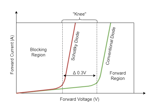
The metal-semiconductor (MS) junction can be biased in forward and reverse directions similar to a conventional PN junction diode. In the forward bias condition, the external voltage source pushes the electrons towards the metal electrode. The electrons flow from N-type to metal compound and constitute majority carriers. The drift current in Schottky diodes is due to these majority electrons. However, in the reverse bias condition, there is no current flow due to the absence of P-type semiconductor material. The absence of minority carriers (holes) gives characteristics of rapid response to the biasing change and current quickly to halt/stop. This leads to the fast switching action of the Schottky diode and demonstrates a basic rectification technique. The characteristic of a typical Schottky diode is shown in the following figure. It is eminent from the figure that the knee voltage of a Schottky diode is much lower compared to a conventional diode. However, the characteristic curve is similar to that of the conventional diode in the forward region only. A difference of around 0.3 V exists between knee voltages of a conventional and Schottky diode.
The low voltage drop across the Schottky diode produces more forward current and that may be multiple of a typical PN junction diode current. As discussed before, the voltage drop across the Schottky diode depends on the metal compound mainly and could offer a variety of voltage drops depending on the metal compound. The lower voltage drop causes less power drop (V x I) across the diode even though the current has increased and as such the heating due to power loss also reduces. All these properties, make Schottky diodes suitable for applications requiring low voltage drop and high current such as in solar panels which have been discussed in a previous article.
The Schottky diodes are expensive due to metal-semiconductor construction compared to that of PN junction diodes of the same ratings. The commercially available Schottky diode series is 1N568xx with a 1-ampere current rating.
An ohmic contact is a form of Schottky diode where the N-type semiconductor is heavily doped in order to reduce contact resistance significantly. This also leads to more linear and non-rectifying characteristics. The ohmic contacts are used to connect semiconductor wafers with the external wires, circuits, or systems. The pins of the dual-in-line (DIL) package are an example of ohmic contacts which connect semiconductor wafers of the chip with an external circuit.
Schottky Diodes based Logic Gates
There are many integrated circuit families available in the market to perform logic operations such as Bipolar, CMOS, and BiCMOS, etc. The bipolar family uses bipolar devices such as diodes and transistors for the logic circuit operations. The Schottky diodes are found in 74 series of bipolar logic families. The conventional transistor-based TTL logic circuit suffers from power loss and slow switching speed. The inclusion of Schottky diode as clamping diode has brought low power loss, high-frequency response, and reduced switching time to logic circuits.
There many subfamilies of bipolar TTL logic circuits which include the Schottky diode and a few of them are listed below:
- 74S – Schottky (High Speed): The Schottky diode is used as a clamp at the base-collector junction of TTL to prevent charge storage/ saturation. This arrangement, compared to the 74 and 74H series, gives faster operation but costs higher and dissipates more power.
- 74LS – Low-power Schottky: This series is based on the 74S series but manufactured to offer lower power loss at a slower switching speed. They tend to give a 10ns gate delay with 2mW of dissipation.
- 74AS – Advance Schottky: This is the improved version of the 74S series. It includes “miller killer” circuitry to offer greater speed at high power consumption. The low-to-high transition gate delay is around 1.7ns at 8mW of power loss.
- 74ALS – Advanced low-power Schottky: This is an improved version of the 74LS series and gives reduced power dissipation at slightly slow switching action. They have 4ns of gate response and 1.2mW of power loss.
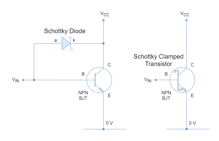
The aforementioned families include a Schottky clamped to a transistor to prevent charge storage or to prevent saturation of the transistor. The prevention of a transistor to operate in saturation gives decreased propagation delay time. It is known that the increase in base current drives the transistor towards saturation and the response may gradually get delayed. The placement of the Schottky diode across the Base – Collector prevents driving of transistor into saturation. When the transistor is operating in the active region then the collector-base junction is reverse biased and as such the Schottky diode. However, an increase in base current leads to the development of voltage across the Schottky diode and drives it to operate in the forward region. This clamps the base-collector junction to Schottky diode knee voltage i.e. 0.4V and would prevent saturation of transistor by shunting excess current through the diode itself.
Conclusion
- The Schottky diode is a solid-state semiconductor device formed by bonding the metal electrode with the N-type semiconductor.
- The metal-semiconductor (MS) junction has no depletion layer around it and this characterizes the Schottky diode with fast switching response and reduced forward voltage drop.
- The MS junction Schottky diodes have forward voltage drops in the range of 0.2 to 0.4 volts which are much lower than the forward voltage drops produced by conventional PN junction diodes (0.6 to 0.9 volts for Silicon diodes).
- Contrary to PN junction diodes, the leakage current in Schottky diodes is much greater and they have much lower breakdown voltages.
- The Schottky diodes are used in applications requiring high current, low forward voltage drop, and reduced switching time such as in digital circuits, renewable energy sources and solar panels, etc.
- The Schottky diodes are used in bipolar logic circuits because of their fast-switching response which is in few nanoseconds (ns) and their reduced power dissipation capability. The subfamilies of bipolar TTL logic which are based on Schottky diodes are 74S, 74LS, 74AS, and 74ALS.
- All subfamilies, 74S, 74LS, 74AS, and 74ALS, use Schottky diode clamped to the transistor and the main difference amongst these subfamilies is the tradeoff between switching time & power dissipation. However, the most commonly used TTL subfamily is 74LS.
- The MS junction is also used as an ohmic contact and for this purpose, a heavily doped N-type semiconductor is used. The resistance of the MS junction is significantly reduced for ohmic contact. The response of the MS junction becomes linear and is used in integrated circuits to connect semiconductor wafers with the external world.


