Skip to content
Android APP
Contact Us
login
/
register
Upload
Primary Menu
Primary Menu
Home
Projects
Audio
Arduino & Raspberry
Automotive
Game – Robots
MCU Development
Microcontroller
Miscellaneous
Motor Control
Modules
Light – Power Control
Oscillators – Timers
PC Related
Power
RF Circuits
Science
Sensors – Detectors
Test – Measurement
Downloads
Android
Audio Software
CAD/CAM Software
Calculators / Info
Design / Simulation
PC Measurements
Microcontrollers
Miscellaneous
PCB Design
Smartphone
Articles
CAD Tools
Calculators
Search Parts
Upload BOM
CAD Models
Community
QA
Blog
Eshop
Home
My account
Wishlist
Cart
Checkout
PCB Assembly
PCBONLINE
PCB assembly service
Box Build Assembly
Search Parts
Search for:
TRENDING:
ESP32
ESP32-P4
ESpressif
eSATA
HAT
Home
Projects
Projects
Light - Power Control
Light - Power Control PROJECTS
Generic selectors
Exact matches only
Search in title
Search in content
Post Type Selectors
project
Filter by Categories
3D Printing
AI
Arduino
Audio
Basic Electronics
Books
Control
DIY
Ebay
Electronics-Lab
FPGA
GPS
Hardware
High Voltage
IC
Interface
IoT
Laser
LCD/OLED/ePaper
Led
Light
Mcu
Miscellaneous
Motor
Parts
PCB
Photovoltaic
Power
Power supply
Products
Raspberry Pi
RF
Robots
SBC
Science
Sensor
SoC-SiP
Software
Soldering
SoM-CoM
Technology
Test Equipment
Test/Measurements
Timer
Tools
Top Stories
Uncategorized
USB
Websites
Youtube
Grid View
List View
Newest
Oldest
Most Viewed
Most commented
Recently Updated
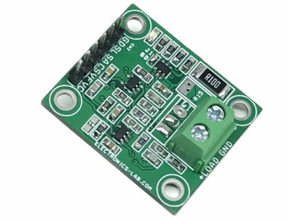
I2C DAC Controlled Electronic Load – Battery Performance...
66
Views
0
Tested
Half-Bridge with Ultra-Precise Current Sense Feedback for Sole...
77
Views
0
Tested
Xenon Flash Tube Driver
61
Views
0
Tested
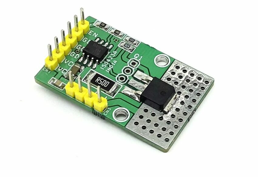
Solenoid, Relay, Valve Driver with Current Regulation
96
Views
0
Tested
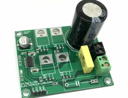
Self-Oscillating Full-Bridge Using IRS2453
339
Views
0
Tested
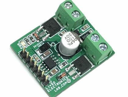
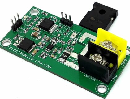
DC Electronic Load – 1A
101
Views
0
Tested
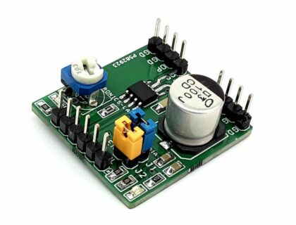
Linear Current Source LED Driver with Dimmer Input
202
Views
0
Tested
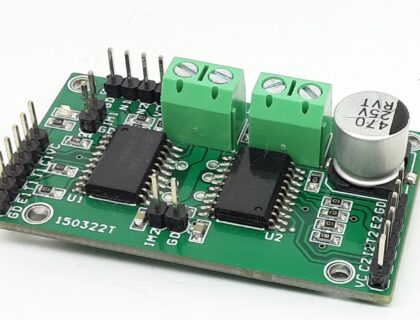
55V – 3A Half-Bridge Power Driver Module
151
Views
0
Tested
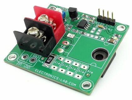
Dual 2A Power Amplifier Module for TEC
137
Views
0
Tested
Electronic DC Load using TLE2141
119
Views
0
Tested
Pages:
1
2
3
4
5
6
7
8
9
10
11
»
TOP PCB Companies