Analog To Digital Conversion – Practical Considerations
In the previous articles about A/D conversion, we considered the concepts of ‘sampling’, ‘quantization’, and ‘binary encoding’ as building blocks of a PCM system. Now, we review those concepts from a practical perspective.
In the previous articles about A/D conversion, we considered the concepts of ‘sampling’, ‘quantization’, and ‘binary encoding’ as building blocks of a PCM system. Now, we review those concepts from a practical perspective.
To perform the analog-to-digital conversion, the first stage is ‘sampling’. There are different regular sampling methods:
- Ideal Sampling: In ideal Sampling, the analog signal is sampled instantaneously by sampling impulses with near-zero durations. This is an ideal method that is usually considered in the theoretical model of sampling and cannot be easily implemented. We have already considered it.
- Flat-top sampling: In this sampling technique, the analog signal is sampled instantaneously by sampling pulses with finite durations and the top of the samples remains constant by using a circuit. This is the most commonly applied sampling method.
In practical ADCs, the quantization and the binary encoding procedures take a finite amount of time, which is called conversion time. This is the time required by the ADC to perform a complete conversion process. For ultimate accuracy, then, it is important that the measured input waveform does not change and hence, the sampled signal amplitude has to be held constant during the conversion interval. To do this, specialized sub-circuits called Sample-and-hold (S/H) are used which can be logically represented in Figure 1.
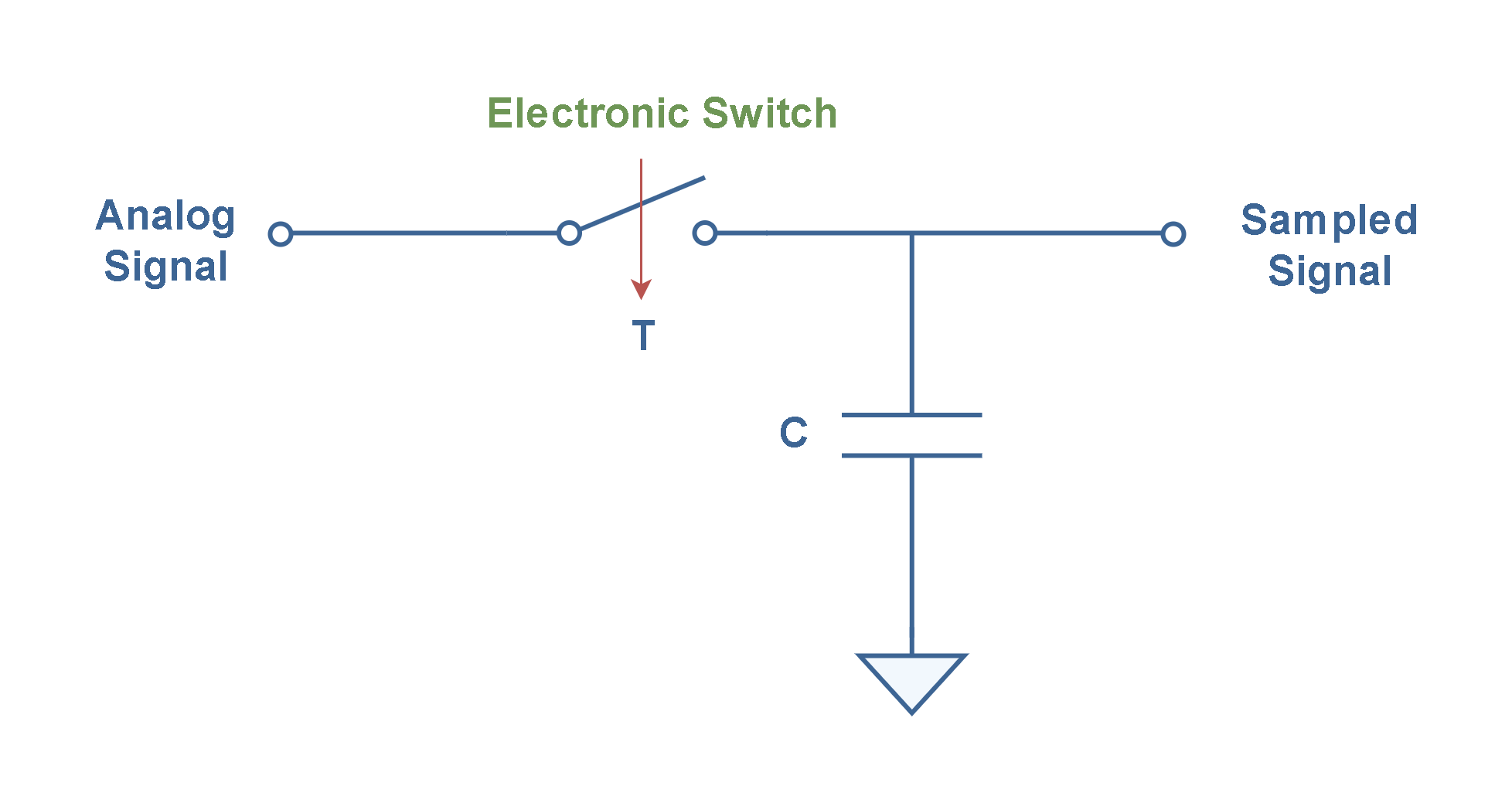
The electronic switch may be a relay, a bipolar transistor, a FET, or a MOSFET controlled by a gating signal. The capacitor holds the sampled measurement of the analog signal for at most ‘Tc’ seconds while a quantized sample is available as an n-bit binary code at the output of the analog-to-digital converter. Obviously, conversion time (Tc) is less than the sampling period (T).
In order to create an S/H, a pair of high-impedance buffers are normally used, along with an electronic switch element and a capacitor to hold the charge. A more realistic sample-and-hold circuit is shown in Figure 2.
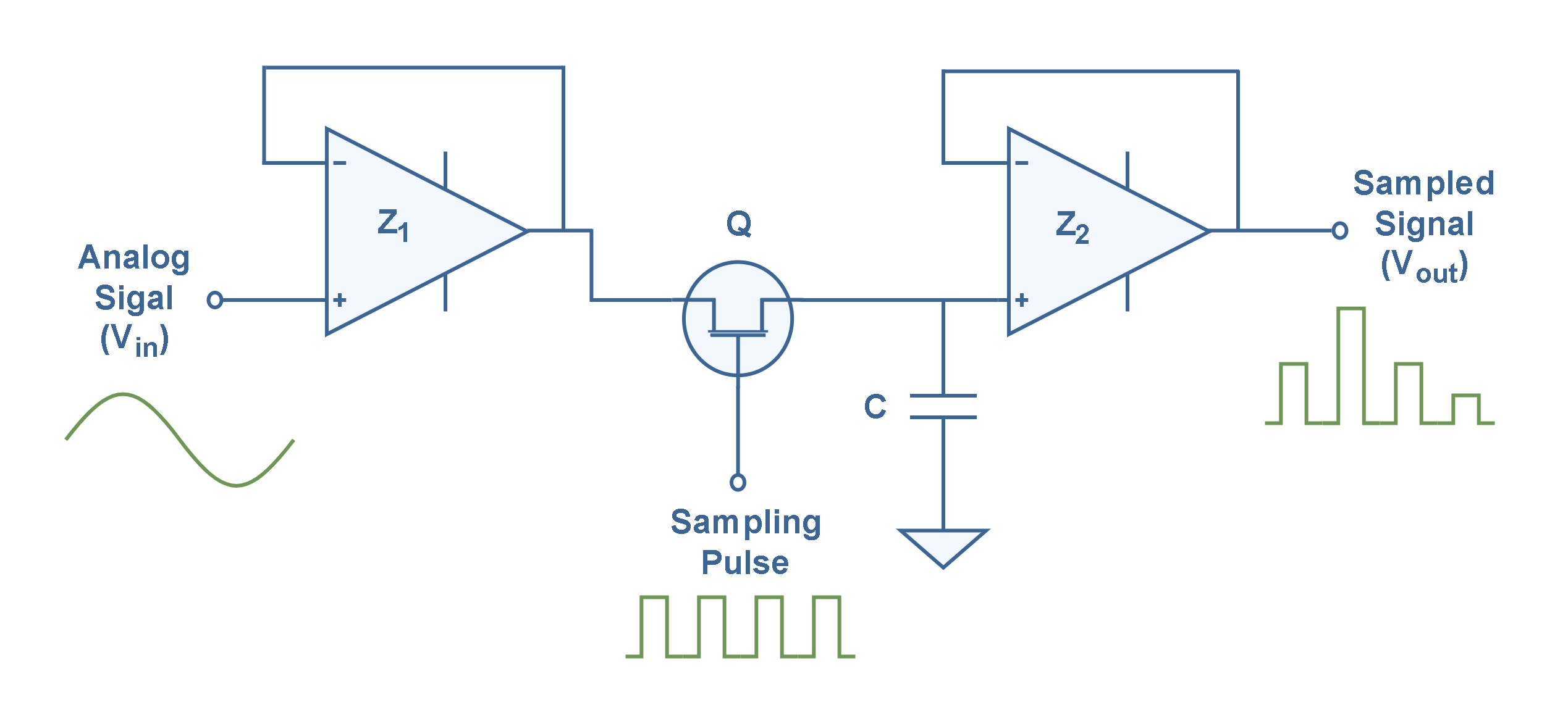
In this mechanism, the voltage-follower configuration is used as a building block which is a special case of an op-amp circuit. As shown in Figure 3, in a voltage-follower configuration, all of the output voltage is fed back to the inverting (-) input of the op-amp by a straight connection. The input signal is also inserted into the noninverting terminal of the op-amp.
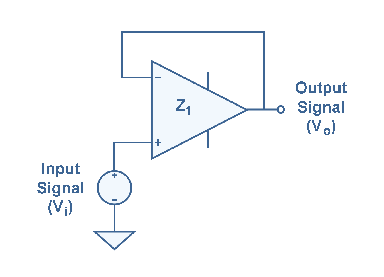
In this configuration, the straight feedback loop has a voltage gain of 1. Then, the overall closed-loop voltage gain of a noninverting amplifier is 1 as explained in Equation 1.

The most important features of the voltage-follower configuration are its very high input impedance and its very low output impedance. These features make it a nearly ideal buffer amplifier for interfacing high-impedance sources and low-impedance loads.
In the Sample-and-hold (S/H) mechanism in Figure 2, the MOSFET element (called Q) acts as a simple switch controlled by the gate terminal. When Q is turned on, it provides a low-impedance path to store the analog voltage sample across the capacitor C. When Q is off, the capacitor C does not have a complete path to discharge through and, hence, keeps the sampled voltage.
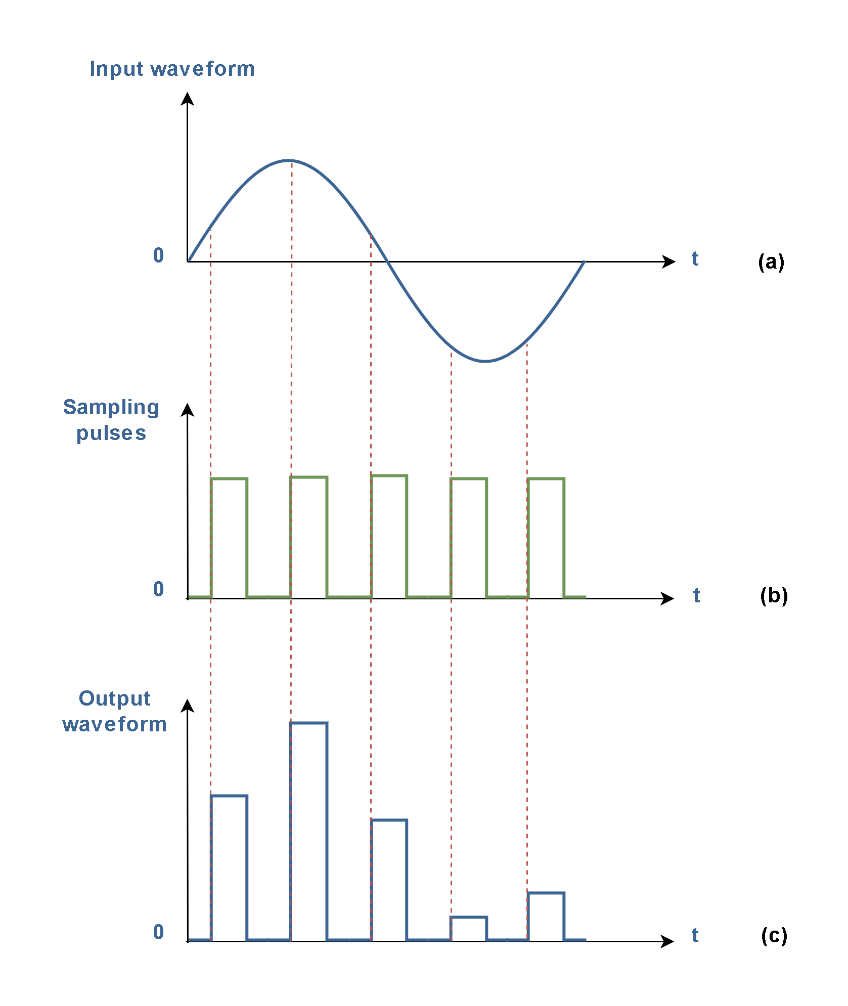
Figure 4 shows the waveforms of the flat-top sampling method. The name comes from the shape of the final waveform.
A sample-and-hold (S/H) system is available on a single monolithic chipset in the market, with the storage capacitor added externally.
FLASH A/D CONVERSION
After converting the analog signal from continuous form to a discrete-time signal (with a mechanism like S/H circuit in Figure 2), it is possible to convert it to digital form by an ADC method. There are several types of ADCs used in different applications. One of the famous circuit configurations for A/D systems is the Flash Conversion method which is generally used for high-speed tasks, such as video applications in which hundreds of megahertz sampling rates are common today.
The Flash ADC utilizes comparators in its mechanism. Essentially, an analog comparator has two input voltages V1 and V2, and one output voltage Vo. it can be implemented by an open-loop op-amp circuit as shown in Figure 5.
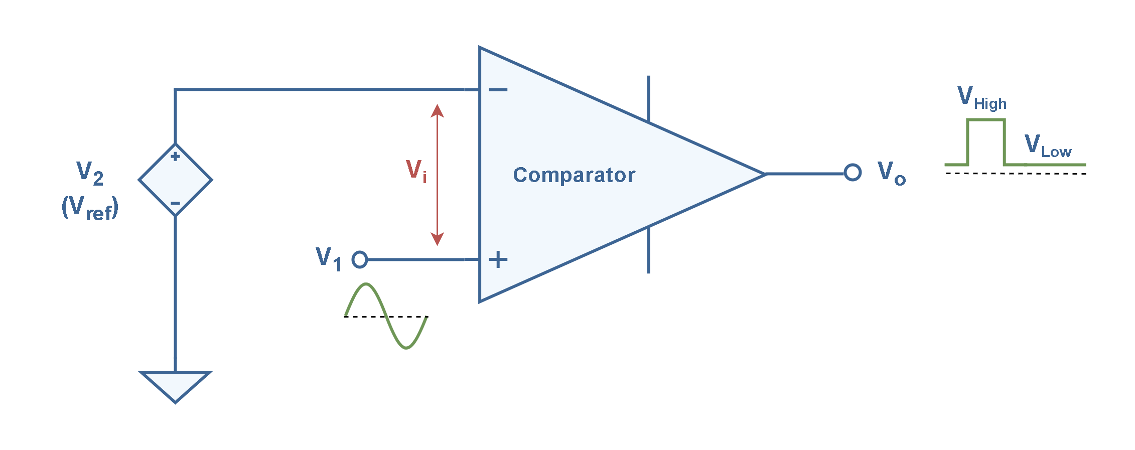
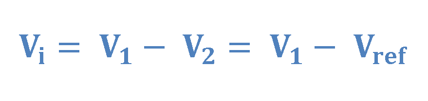
Often, one input (V2) is a constant reference voltage (Vref), and the other is a time-varying signal (V1). As Equation 2 explains, the input signal of the comparator (Vi) is the difference between the 2 signals of V1 and Vref.
The ideal comparator has the voltage transfer characteristic shown in Figure 6.
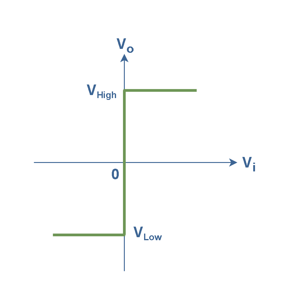
Clearly, the input is compared with the reference and the output equals one of two states, VLow or VHigh. It has a constant output voltage Vo (= VLow) if Vi < 0 and a different constant voltage Vo (= VHigh) if Vi > 0. Equation 3 explains it.

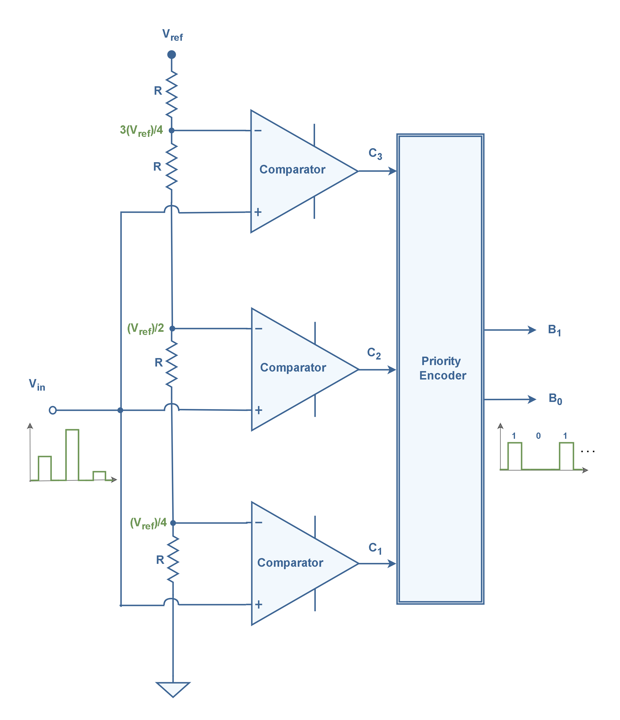
The block diagram of a simple 2-bit flash ADC is shown in Figure 7. The circuitry of a Flash ADC consists of a precision resistor ladder network which is connected to a set of analog comparators, and a binary priority encoder. The priority encoder is a combinational logic device (including logic gates) that produces a binary number on its output representing the highest value input.
AD
The input signal (Vin) is passed to a number of analog comparators in parallel i.e., a bank of operational amplifiers. A reference voltage source (Vref) supplies the resistive voltage-divider network and a threshold voltage (Vth) for each comparator is set by this network. Effectively, there is one comparator for each level.
The input signal serves as one of the inputs to each of the comparators which is connected to the noninverting terminal of op-amps. The second input for each of the comparators, connected to the inverting terminal of op-amps, is a threshold voltage (Vth), different for each comparator.
The input voltage signal to be digitized is applied to all of the comparators simultaneously. Hence, the input voltage will be compared to all threshold voltages simultaneously. The analog comparators indicate whether or not the input voltage is above or below the threshold at each level. If the input signal level (Vin) on the positive input of a comparator is greater than the level of the negative input, the output will be ‘High’. Otherwise, the comparator outputs a ‘Low’ voltage.
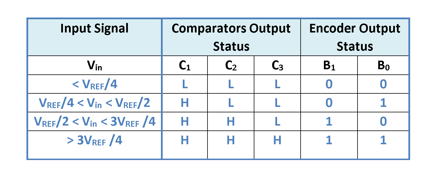
When a given signal is applied, a number of comparators (towards the bottom of the string) in which Vin is greater than their references, will produce a VHigh. Conversely, the comparators (towards the top) will indicate a VLOW. The set of comparator outputs is fed into a priority encoder that will turn this simple sequence (C1 C2 C3) into a normal binary word (B1 B0). The final 2-bit codes are the digital equivalent of the input original analog signal. The bits at the output of the coding network can then be entered into a flip-flop register for storage.
For an n-bit converter, we usually need 2n resistors with equal resistances. The number of bits the flash ADC produces per each binary word (n), determines the number of comparators used. The number of comparators needed for n-bit A/D conversion is calculated by Equation 4.

For example, a 4-bit flash ADC would require 24 – 1 = 15 comparators to implement.
The structure of the circuit in Figure 7 can be extendable for a higher number of bits. Threshold voltages (Vth) for each comparator can be found by Equation 5.
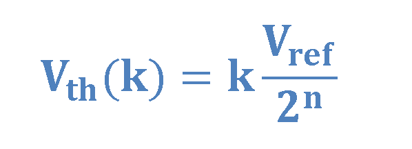
where k is the index number of the threshold voltage.
Referring to the circuit in Figure 7, for the present case of a two-bit A/D converter (n=2), the threshold voltages of the three comparators will be Vref/4, Vref/2, and 3Vref /4. The output status of various comparators depends upon the input signal Vin. For instance, when the input level Vin lies between V/4 and V/2, the C1 output status is High whereas the C2 and C3 outputs are both Low. The final results of the priority encoder are summarized in Truth Table 1.
In practice, the op-amp should have good stability against temperature changes and supply voltage variations.
As the main advantage, flash ADCs are the fastest converters because the internal comparisons are performed in parallel and at the same time.
As the main disadvantage, the complexity of the hardware will be increased for large word lengths. Firstly, the resistors in the voltage divider chain have to be matched and manufactured with high precision for accuracy. Secondly, the number of comparators grows fast as the number of bits is increased. For example, to build a flash ADC circuit with 8 bits, we need to have 255 (= 28 – 1) comparators! Also, the power dissipation of the circuit will be considerable.
Therefore, they are limited in the number of bits they can accommodate. Generally, flash converters are limited to 4-bit up through 10-bit digital output word lengths.
Summary
- Voltage-follower is a closed-loop, noninverting op-amp with a voltage gain of 1.
- In this designation, the op-amp will not draw current from the signal source and will not load down it because of its very high input resistance.
- The storage time of the capacitor is called the A/D conversion time because it is during this time that the ADC converts the sample voltage to a binary code.
- The primary benefit of an S/H amplifier is that it stores the analog voltage during the sampling interval. The S/H amplifier, however, stores the voltage on the capacitor; with the voltage constant during the sampling interval, quantizing will then be accurate.
- Parallel ADC or Flash converter – uses many comparators connected in parallel, each with a different reference voltage. The outputs of these comparators are then inputted into a priority encoder. This encoder provides a binary output based on which comparator outputs are high and which are low.
- The voltages tapped from the terminals of the resistors, which establish threshold voltages for each allowed quantization level, are then compared with the input voltage.
- The threshold voltages to be used for comparators are in general Vref/2n, 2Vref/2n, 3Vref/2n, 4Vref/2n, and so on. Here, Vref is the maximum amplitude of the analog signal that the A/D converter can digitize, and n is the number of bits in the digitized output.
- Flash-type (or parallel) ADCs are the fastest due to their short conversion time and can therefore be used for high sampling rates.
- In this system, an 8-bit flash A/D converter requires 255 comparators. The cost of long word length A/D comparators escalates as the circuit complexity increases and as the number of analog comparators rises by 2n – 1.
- On the other hand, the larger the n, the more complex is the priority encoder. So, it is difficult and expensive to build the circuit for large word lengths. Thus, they have limited word length (10 bits or less).


