Analog To Digital Conversion – Performance Criteria
Overview In this series of articles, we considered PCM (Pulse Code Modulation) as a method of digital representation of an analog signal. In the PCM method, the samples of the continuous wave are allowed to take only certain discrete values.
Overview
In this series of articles, we considered PCM (Pulse Code Modulation) as a method of digital representation of an analog signal. In the PCM method, the samples of the continuous wave are allowed to take only certain discrete values. These amplitudes are then assigned a code, where each code uniquely represents the magnitude of the sample. These code words as digital data find application in various contexts.
Analog-to-digital converters (ADCs) are devices or circuits that practically transform analog signals into digital ones using the PCM concept. They have many applications in the industry. For example, many modern microcontrollers are equipped with built-in ADC converters. This allowed designers to interface easily with analog sensors, convert analog signals from the environment into digital data, and process it within the microcontroller for various applications.
The process of analog-to-digital conversion can be executed through various architectures, such as successive approximation register (SAR), parallel (flash) conversion, sigma-delta conversion, and more.
The task of the digital-to-analog converter (DAC) is the inverse of the ADC: it converts numerical digital values back into continuous analog signals. DACs are employed to translate the outcomes of digital processing into real-world variables for control, information display, or other forms of analog processing. Figure 1 illustrates a general block diagram of a digital processing system.
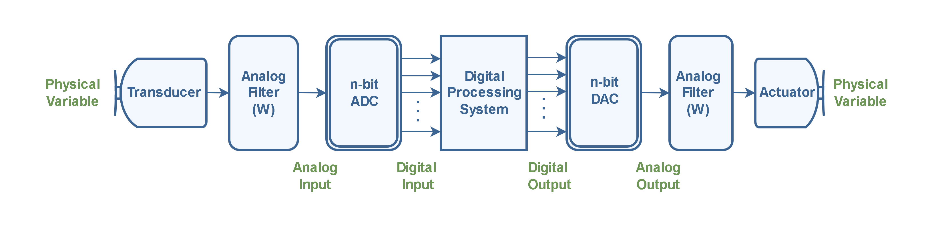
Analog quantities are often representative of real-world phenomena. In this configuration, the primary variable typically relates to a physical parameter like temperature, light, etc., which is transduced into electric voltages or currents by a transducer.
Here, analog filters are used to comply with the sampling theorem. The first filter placed before the ADC is an LPF called an anti-alias filter. This filter, placed prior to the ADC, eliminates frequency components above half of the sampling rate (fs/2) that could lead to aliasing during sampling. The filtered analog signal is then transformed into digital codes by the ADC block and directed into the digital processing system, which could be a microcontroller or other forms of data processing and manipulation.
After that, the processed digital signal is fed to the DAC stage to convert it back into an analog signal. The second filter placed after the DAC block is also an LPF and is called a reconstruction filter. It also removes frequencies above the Nyquist rate (fs/2). Finally, the analog output signal is transduced back to the physical world by an actuator stage for any further physical operations.
As an example, in an audio signal processing configuration, an ADC converts the analog audio signal captured by a microphone, into a digital signal for computer-based sound effects processing. The DAC then converts the processed digital signal back into analog form, which can be played through a loudspeaker.
In contemporary electronics, instrumentation, information technology, data acquisition and transmission, control systems, medical imaging, professional and consumer audio/video, and computer graphics, converting analog signals to digital has become a fundamental process.
In this article, we explore the key performance criteria that define the effectiveness of ADCs in their applications.
Quantization Errors
There are various sources of errors in conversion circuits. Among them, quantization error (Qe) or quantization uncertainty stands out as one of the most critical factors that significantly impact the performance of A/D or D/A converters.
Quantization errors occur in analog-to-digital conversion when the continuous analog signal is approximated by discrete digital values. In a PCM encoder, every voltage sample is already rounded off (quantized) to the nearest available level and then translated into its corresponding binary code. When the code is converted back to analog at the decoder, any round-off errors are reproduced.
Theoretically, the conversion will never be 100% accurate; that is, a finite amount of information will be lost forever during the conversion process. It means when the digital representation is converted back to analog, the result will not be identical to the original waveform.
Let’s refer to Figure 2 as the block diagram of a 3-bit A/D converter.
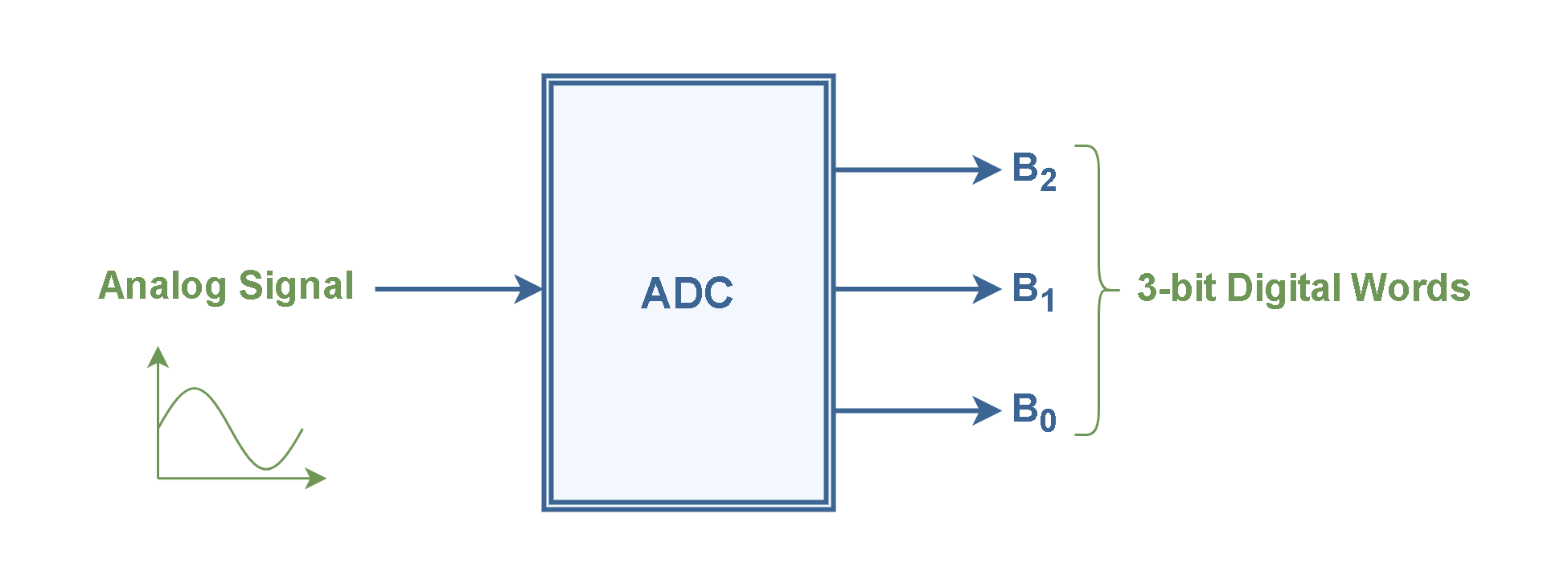
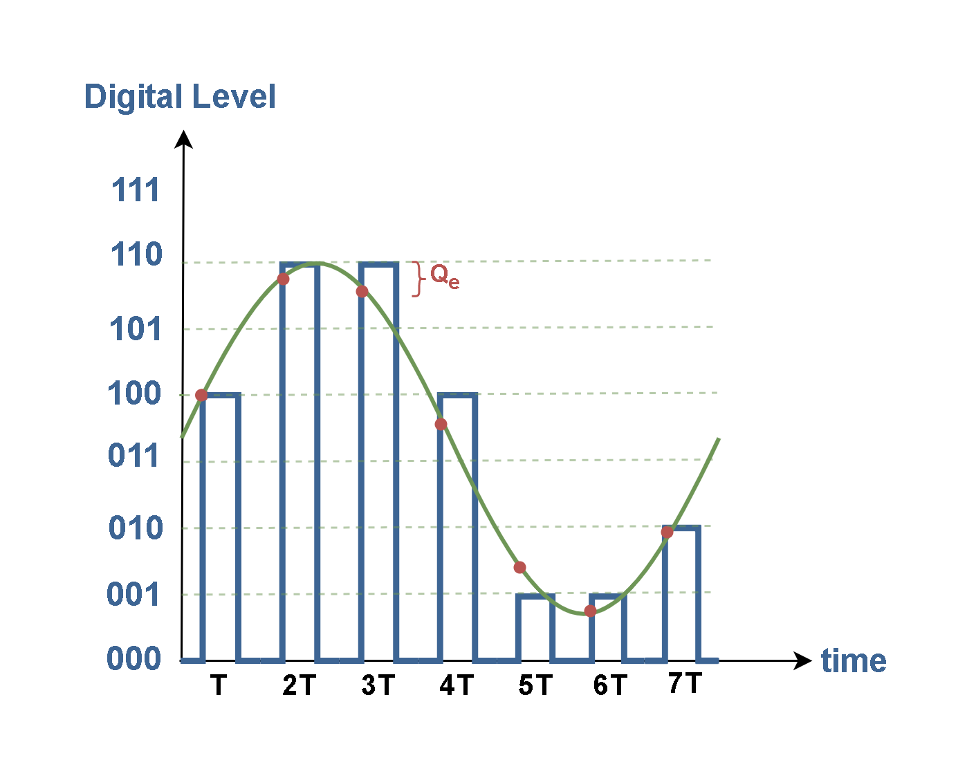
Obviously, a 3-bit ADC has 8 digital (quantum) levels. The output digital results of this system in comparison to the analog input, are represented in Figure 3 and a typical sample of Qe is indicated on the graph.
Now, we may look at the effects of quantization. Figure 4 shows the transfer characteristics for a 3-bit unipolar ADC with a full-scale voltage of 1 volt.
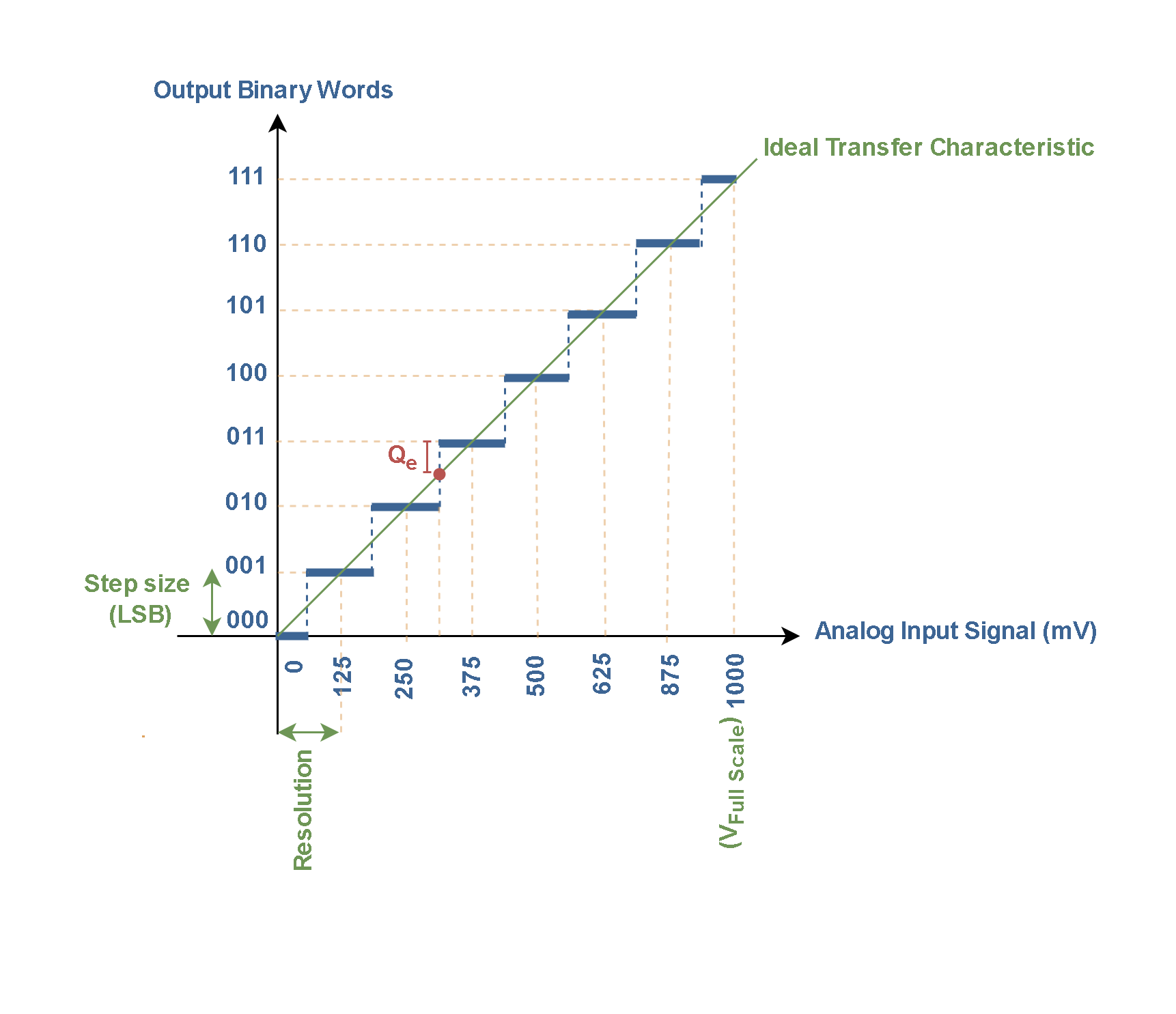
Figure 4 represents a 3-bit quantizer, which maps a range of analog input values to only eight (23) possible output digital values. If the maximum peak-to-peak value of the input signal is 1 V, each step in the staircase has (ideally) the same size along the y-axis, which is defined as 1 LSB (the least significant bit) in terms of voltage. In this case, 1 LSB is equal to 1/8 V (or 125 mV).
Under these conditions, as an example, it would be impossible to perfectly encode a value of 300 mV. The nearest value available would be binary 010, which yields 250 mV. Obviously, the resulting round-off creates some error in the digital representation.
In an ideal assumption, the characteristic of the conversion system could be a straight diagonal line with no steps at all. But in reality, an ADC quantizes a sampled signal by selecting a single discrete value from a pre-established finite list of such values to represent each analog input sample. This rule gives the transfer function of analog input to digital output a uniform ‘staircase’ characteristic.
The vertical difference between the actual analog value and the quantized digital value at each sample point defines the quantization error (Qe). The graph of quantization errors in Figure 5 is resulted from the subtraction of ideal values of the linear function from the actual values of the staircase function. The maximum magnitude of the quantization error equals half of a quantum level (q/2) where q is the width of an individual step. Then, Qe can fluctuate within the range of ± (1/2) LSB or ± (q/2) as illustrated in Figure 5.
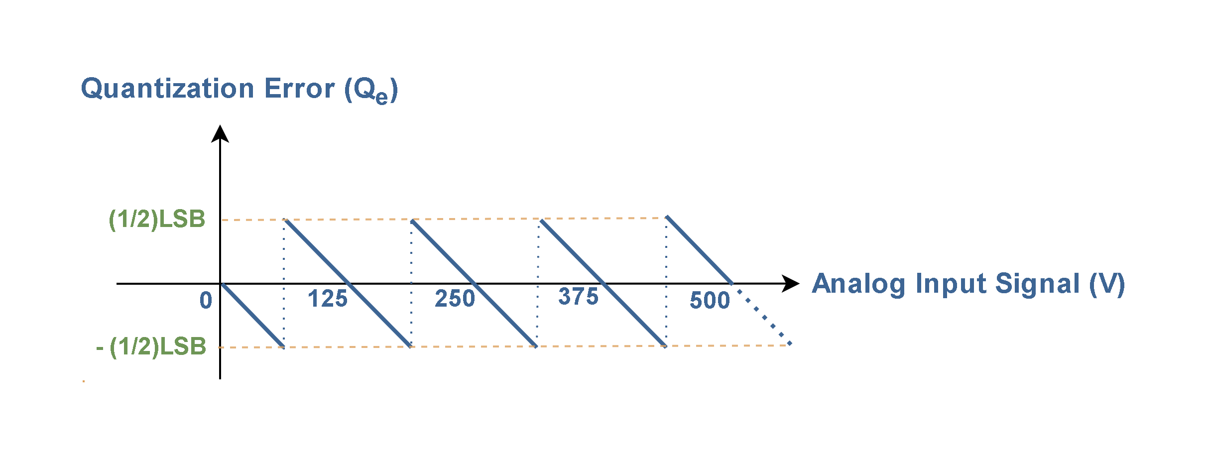
The result is a sawtooth-pattern error voltage that manifests itself as white noise added to the analog input signal. The quantization error is an actual voltage, as it alters the signal amplitude. Consequently, the quantization error is also referred to as the quantization noise (Qn).
The quantization error is generally larger when the number of bits used for conversion (n) is small, as there are fewer quantization levels to represent the continuous signal accurately. As the number of bits increases, the quantization error becomes smaller, resulting in a more accurate representation of the original analog signal. In practical terms, it is possible to reduce the error to such small values that it may be ignored in many applications.
The Signal-to-Quantization Noise Ratio (SQNR) is a measure of the ratio between the power of the original analog signal (Ps) and the power of the quantization noise (Pqn) introduced during the analog-to-digital conversion. However, it is assumed that the ADC is relatively free of random noise and that the transitions can be easily measured.
Then, the Signal-to-Quantization Noise Ratio (SQNR) can be generally calculated in terms of dB using Equation 1.

In an ideal n-bit converter scenario where the input signal is a full-amplitude sine wave, the corresponding SQNR can be determined using Equation 2.

This gives the ideal value for an n-bit converter and shows that each extra 1 bit of resolution provides approximately 6 dB improvement in the SQNR.
SQNR is a valuable metric for assessing the quality of the analog-to-digital conversion in contrast to the quantization error. A higher SQNR value indicates better accuracy and a smaller impact of quantization noise on digital representation.
A/D And D/A Conversion Performance Criteria
The specifications which impact the performance of an ADC are similar to those for a DAC. In addition to SQNR, some other major factors that determine the performance of D/A and A/D converters are resolution, sampling rate, speed, accuracy and dynamic range. They are explained below.
Resolution: In an A/D system, the resolution is the smallest change in voltage at the input that the system can detect and convert into a corresponding change in the digital code at the output. Similarly, for a D/A circuit, resolution refers to the smallest change in the output analog signal that the circuit can produce.
D/A or A/D IC manufacturers usually specify the resolution in terms of the number of bits in the digital code (n) or voltage corresponding to the least significant bit (LSB) of the system.
Another approach to expressing resolution is by indicating the voltage step magnitude between quantization levels, also termed the quantization width (q). For an n-bit DAC, the LSB carries a weight of 2-n. For instance, an 8-bit DAC can resolve 1 part in 28 or 0.39% of the full-scale output voltage when the binary input code is incremented by one LSB. Then, for full-scale voltage (VFS = Vmax – Vmin) equals 10 volts, the resolution of the 8-bit system is 0.039 (= 10/28) volts.
Generally, it can be calculated in terms of voltage by Equation 3.

Sampling Rate: The sampling rate denotes the frequency at which the analog signal can be sampled and translated into a digital code per unit of time. For proper A/D conversion, the minimum sampling rate must be at least two times the highest frequency of the analog signal being sampled to satisfy the Nyquist sampling criterion. The more samples taken in a given unit of time, the more accurately the analog signal is represented in digital form.
Speed: For A/D converters, the speed is specified as the conversion time, which represents the time taken to complete a single conversion process, including sampling the analog signal, processing, and generating the digital output. In A/D converters, conversion speed, along with other timing factors, must be considered to determine the maximum sampling rate of the converter.
For D/A converters, the speed is specified as the settling time, which is the delay between the binary data appearing at the input and the output voltage reaching a stable value. This sets the maximum data rate that the converter can handle.
Accuracy: Accuracy is the degree of conformity between the converter’s output and the actual analog signal value. The resulting round-off error occurs due to the quantization process, leading to some deviation from the actual analog value.
As the number of bits increases, the step size between quantization levels decreases, leading to higher accuracy when converting between analog and digital signals. For example, an eight-bit word (n = 8) provides 256 distinct values (28) for representation, offering a more precise conversion of the analog signal than using a four-bit word with 16 distinct values (= 24).
Dynamic Range: Dynamic Range refers to the range of signal amplitudes that an ADC can accurately represent in its digital output without significant loss of accuracy. In other words, the dynamic range is the difference between the maximum and minimum input signal levels that the ADC can handle effectively.
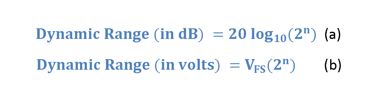
Dynamic range is expressed as the ratio of the maximum input voltage to the minimum detectable voltage and, it is subsequently transformed into decibels. Calculation of the Dynamic Range (DR) is defined in Equation 4, combining logarithmic (dB) and linear (voltage) aspects.
The full-scale voltage (VFS = Vmax – Vmin) is the voltage range that the ADC uses to represent the analog input signal.
For example, if the ADC uses a reference voltage of Vref = 5 volts, the input voltage should fall within this range for accurate conversion. For a 12-bit ADC (n = 12) and the reference voltage of 5 volts, the dynamic range can be assessed as follows:
Dynamic Range (in dB) = 20 log (212) = 20 log (4096) ≈ 72 dB
or,
Dynamic Range (in volts) = 5 .212 = 5 (4096) = 20480 volts
It is essential to remember that all performance parameters of electronic components, including converters, can be influenced by variations in supply voltage and temperature. Datasheets commonly specify these parameters under specific temperatures and supply voltage conditions to offer standardized information. However, in practical systems, operating conditions may deviate significantly from the specified figures. As a result, actual performance can differ from what is outlined in the datasheet.
Summary
- The real-world analog input to an ADC is a continuous signal with an infinite number of possible states, whereas the digital output is, by its nature, a discrete function with a finite number of different states.
- An ADC is a device that performs PCM. It samples and translates an analog signal into a digital format, where each sample is represented by a binary code.
- A digital binary code is converted to an analog output (current or voltage) by a DAC.
- Quantization Error (Qe), also known as quantization noise, is the error introduced during the process of converting a continuous analog signal into a discrete digital representation. It is essentially the error caused by approximating the continuous signal with discrete digital values. Obviously, the resulting round-off creates some errors in the digital representation. It results in a deviation between the actual analog value and its digital representation.
- There may be a difference of up to ½ LSB between the actual input and its digital form.
- This error can be reduced by increasing resolution so that finer steps may be detected.
- For A/D circuits, the resolution is the smallest input voltage that is detected by the system. Resolution is the smallest standard incremental change in the output voltage of a DAC. The number of discrete steps or bits that an ADC/DAC can represent, determines its precision in converting analog signals to digital data or vice versa. Typically, the resolution is specified using a number of bits in digital codes (n), although a voltage specification (LSB) is also possible.
- The sampling rate is the frequency at which the ADC samples the analog input signal to convert it into discrete digital data points.
- For A/D converters, the speed is specified as the conversion time i.e., the time to perform a single conversion process. For D/A converters, the speed is specified as the settling time e., the delay between the binary data appearing at the input and a stable voltage being obtained at the output.
- As the number of bits increases, the step size between quantization levels decreases. Therefore, the accuracy of the system is increased when a conversion is made between an analog and digital signal.
- The dynamic range (DR) of an ADC is the ratio of the largest to the smallest signals the converter can represent. It measures the range of signal amplitudes that an ADC can accurately represent in its digital output without significant distortion.


