Analog To Digital Conversion – Decoding Signals
This article details how Digital-to-Analog Converters (DACs) use weighted resistor and R/2R ladder networks to reconstruct analog waveforms from binary data.
Converting Digital Data To Analog Signals
In the previous parts of the article, we considered how to convert an analog signal to digital by the PCM method, as a binary encoding process. Now we want to consider the reverse process as binary decoding. This combination of binary encoding/decoding procedures is an essential part of signal processing in thousands of applications in the industry and the world of technology.
The purpose of digital-to-analog conversion is to take discrete numerical data (which represent an analog signal) as the input and reproduce the original continuous waveform as the output. Digital-to-analog converters (DACs) are used in transforming digital processing data, back to ‘real-world’ values for further analog processing.
Digital-to-analog converters actually perform the role of reconstructing the original continuous electrical waveform. Since DACs in their configuration are much simpler than ADCs (analog-to-digital converters), they are correspondingly cheaper. Figure 1 shows the schematic of an n-bit DAC.
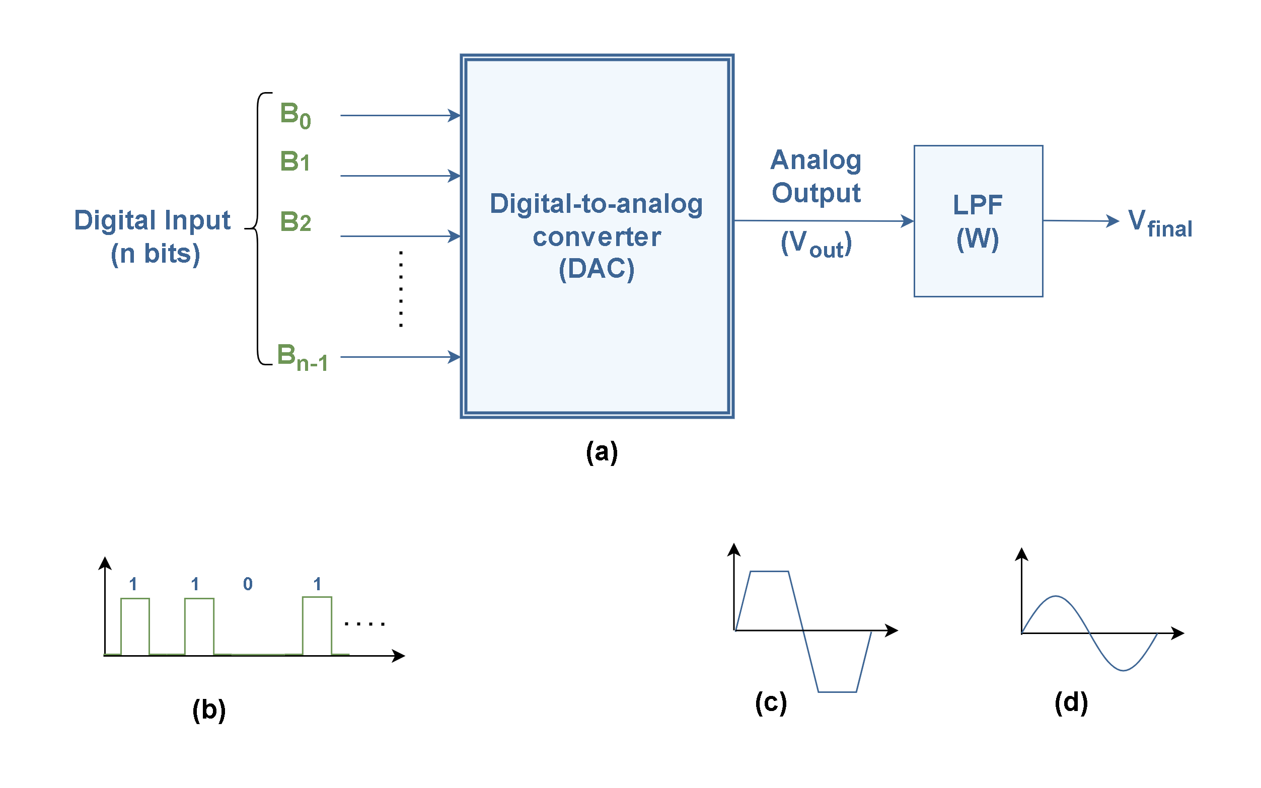
Figure 1 (a) shows the main function of an n-bit DAC system to convert binary words [Bn-1 … B1B0] to analog signals at the output (Vout). The typical input waveform is plotted in Figure 1 (b). Although the output analog signals are usually not perfectly reconstructed, as it shown in the typical waveform in Figure 1 (c), a low pass filter (LPF) is almost always necessary to correct the final waveform to be more similar to the original, as shown in Figure 1 (d).
Reconstruction uf the Original Continuous Signal
There are many applications that require the construction of analog waveforms from the digital sequence of numbers. The most common digital-to-analog converter is multiplying DACs. The name arises because the output is constructed by summation of the products of the binary code values and voltage sources. Each bit of the binary code turns on or off a corresponding voltage source. The sum of all the available voltages produces a resultant voltage for output.
For this purpose, simple resistive networks can be used. Figure 2 shows the concept of converting a three-bit digital input into an analog output by such a resistive network. The resistors are scaled specifically to represent weights for the different input bits. The bits are assumed as electronic switches which may close the circuit while their values are ‘1’ and may also open branches while their values are ‘0’.
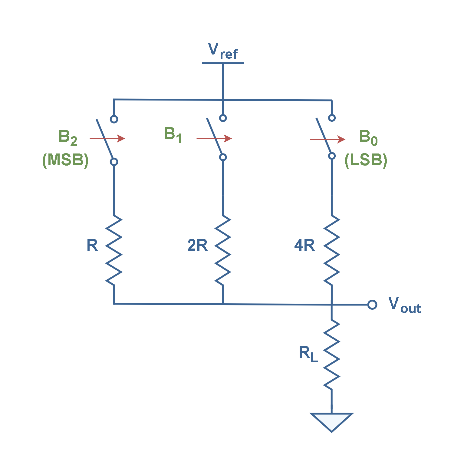
Figure 2 shows the network with a main voltage source (Vref) and three voltage dividers. With the help of simple circuit analysis, like Millman’s theorem, it can be proved that the output voltage is given by Equation 1.
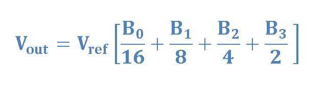
In this expression, B0, B1, and B2 are numerical values of input bits which may be 0 or 1. This expression can be simplified to Equation 2.
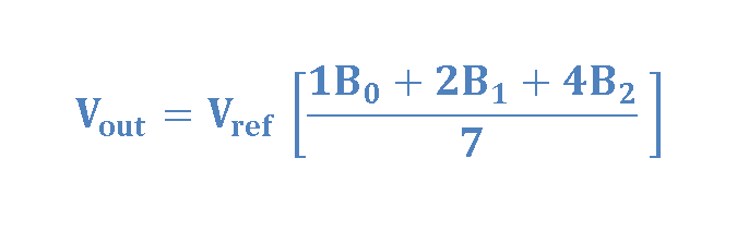
It can be further expressed by considering the weight of bits as Equation 3.
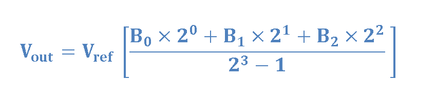
Thus, Vout is a voltage waveform as the counterpart of the digital word of [B2 B1 B0] at the time of exiting this word (T).
The configuration in Figure 2 can be extended to an n-bit weighted resistive D/A converter to get the following generalized expression in Equation 4.
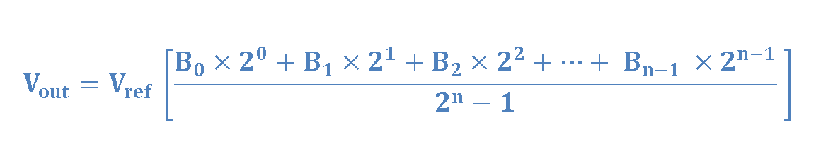
According to Equation 4, a logic ‘1’ at LSB (the least significant bit) position (B0) would contribute Vref /(2n −1) to the output voltage. The contributions of successive higher bit positions in the case of a logic ‘1’ would be 4Vref /(2n −1), 8Vref /(2n −1), and so on. Finally, a logic ‘1’ in MSB (the most significant bit) position would deliver (2n-1. Vref )/(2n −1) to the output, as the most contribution.
When all input bit positions have a logic ‘1’, the maximum analog output is given by Equation 5.
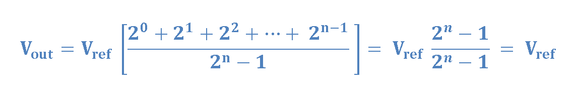
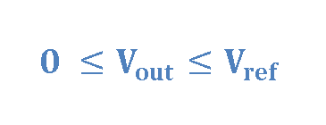
In the case of all inputs being in the logic ‘0’ state, Vout = 0. Therefore, the analog output Vout of the resistive DAC varies from 0 to Vref volts as the digital input varies from an all 0s to an all 1s input. Equation 6 explains the range of the output amplitude Vout .
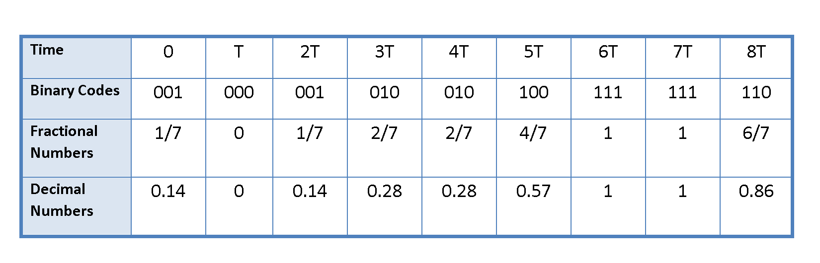
Let’s recall our previous example in the second part of the article:
If we take the results of the ADC conversion in that example as our new input binary data and apply the weighted resistive D/A converter to that binary numbers, the new decimal values result in Table 1 (Vref = 1 V).
Table 1. The decimal output results of DAC corresponding to the digital codes from the previous example.
If we plot the results of Table 1 in terms of time, the original analog waveform is reconstructed approximately as shown in Figure 3.
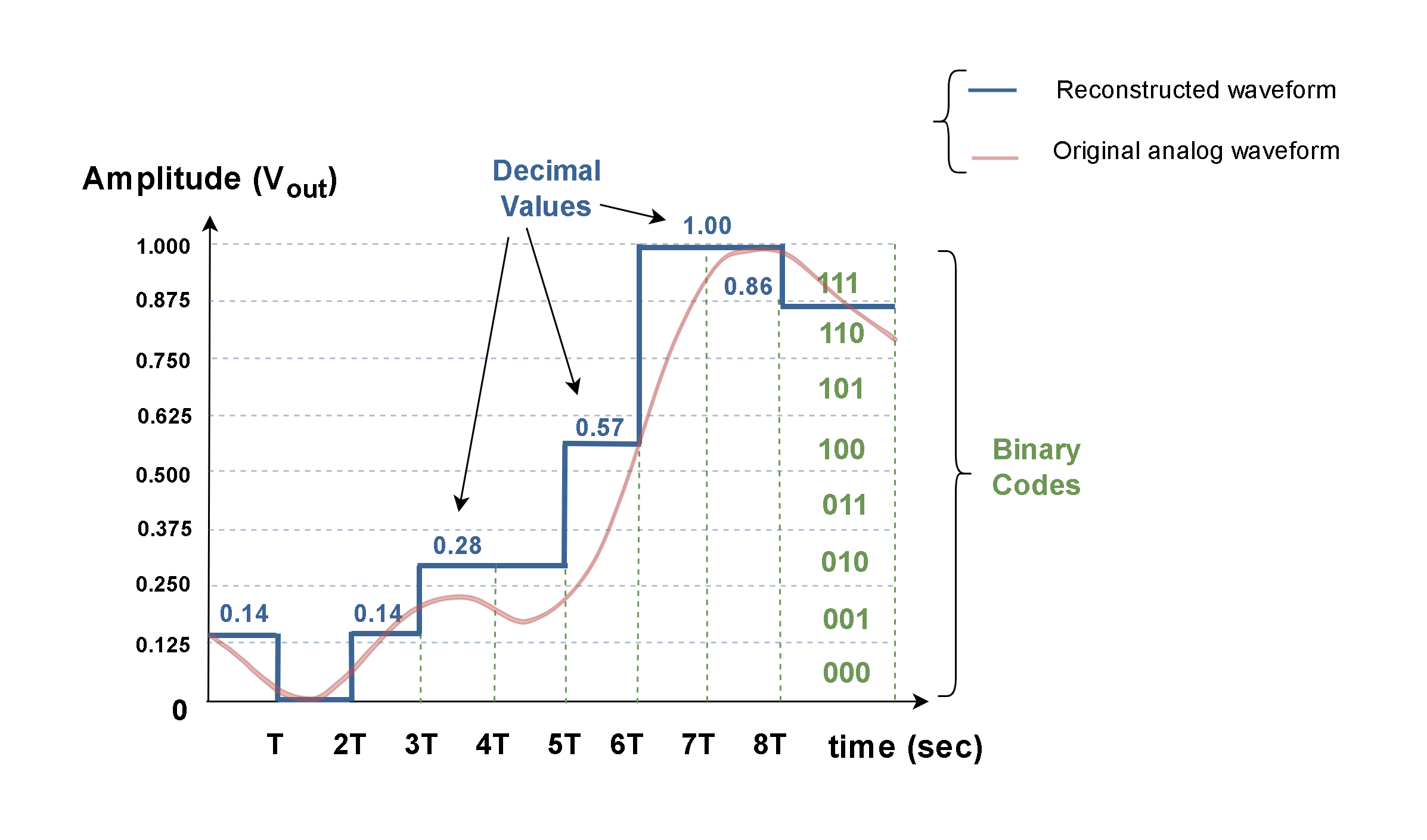
Obviously, this approximation of the original waveform is not perfect! As we have already considered, the precise conversion of analog waveforms to digital (or from digital domain to analog) needs a large number of bits (3-bit words are normally not enough). A better approximation will be achieved by increasing the number of bits (n).
Also, this waveform is before the stage of filtering. To achieve a smoother curve, an LPF is applied after the output in practical DAC systems.
Weighted-Resistor Network for D/A Conversion
Based on the prior resistive DAC concept, Figure 4 shows a more realistic configuration for a DAC circuit utilizing an operational amplifier.
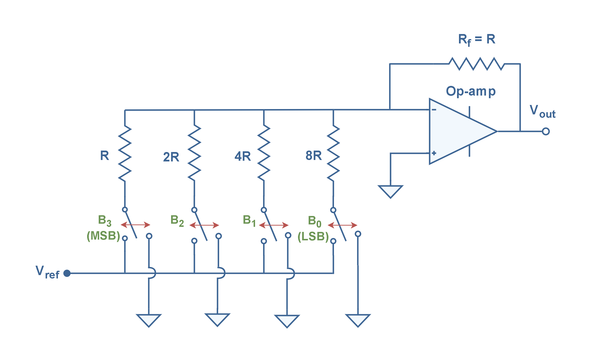
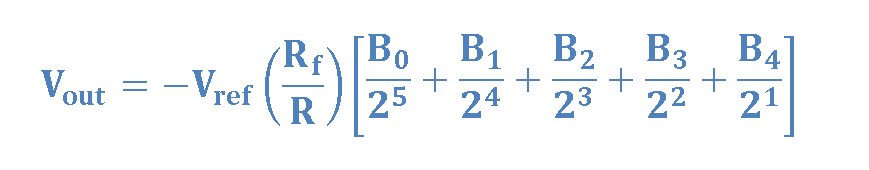
Essentially, this configuration is a weighted-resistor decoder that converts a 4-bit code from digital to analog. The values of resistors are chosen such that the resistance in each branch is double the previous one, i.e. the current reduces by a factor of 2 for each branch or bit path. This arrangement confirms a proper conversion from a binary number to a decimal value. The overall circuit simultaneously uses the ideas of a summing amplifier and an inverting amplifier, with the output voltage Vout.
The voltage source (Vref), as the reference of logic ‘1’ or ‘on’, is applied to a series of scaled resistors. The voltages at one end of the resistors are either switched ‘on’ or ‘off’ relating to the status of input bits as shown in Figure 4. The ‘off’ voltages are grounded to zero and the ‘on’ voltages are summed. The output is proportional to the weighted sum of the input voltages.
The resistor with the lowest value R corresponds to the highest weighted binary input B3 (MSB) with a weight of 23 (= 8). The other resistors with values of 2R, 4R, and 8R respectively correspond to the binary weights of 22 (B2) and 21 (B1), and 20 (B0 which is LSB).
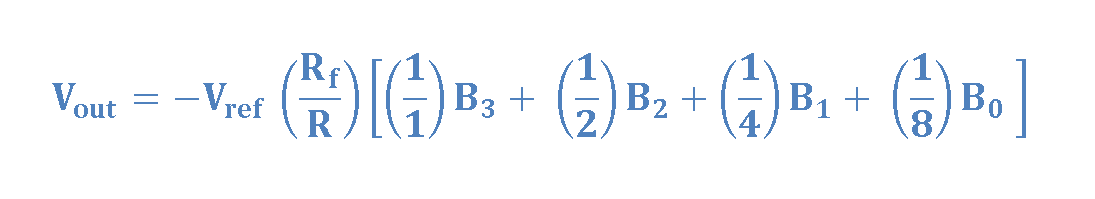
The relationship between the digital input sequence [B3 B2 B1 B0] and the analog output Vout is as Equation 7.
If Vref is originally selected by negative polarity, the positive Vout will be achieved. Some DAC devices have a built-in reference voltage source. Other ones allow the user to provide an external reference voltage, thereby setting the accuracy of the output.
Binary Ladder Network For D/A Conversion
The simple resistive decoder concept of Figure 2 has two serious practical disadvantages:
- Each resistor in this network has a different value. Specifically, there is a large difference in resistor values between the LSB and MSB for a large number of bits (n). Such networks usually use precision resistors. Precision resistors are designed for applications where fitted resistance tolerance and stability are primary considerations. Therefore, such a configuration causes extra expenses.
- The resistor used for the most significant bit (MSB) is required to handle a much larger current than the LSB resistor. So, for a larger number of bits, we need a set of resistors with different sizes and current characteristics.
To overcome these disadvantages, a second type of resistive network called the binary ladder (or R/2R ladder) is used in practice. The binary ladder is also a resistive network that produces an analog output equal to the weighted sum of digital inputs. Here the resistance values span a range of only 2 to 1.
Figure 5 describes the concept of the basic R/2R binary ladder network for a four-bit D/A converter.
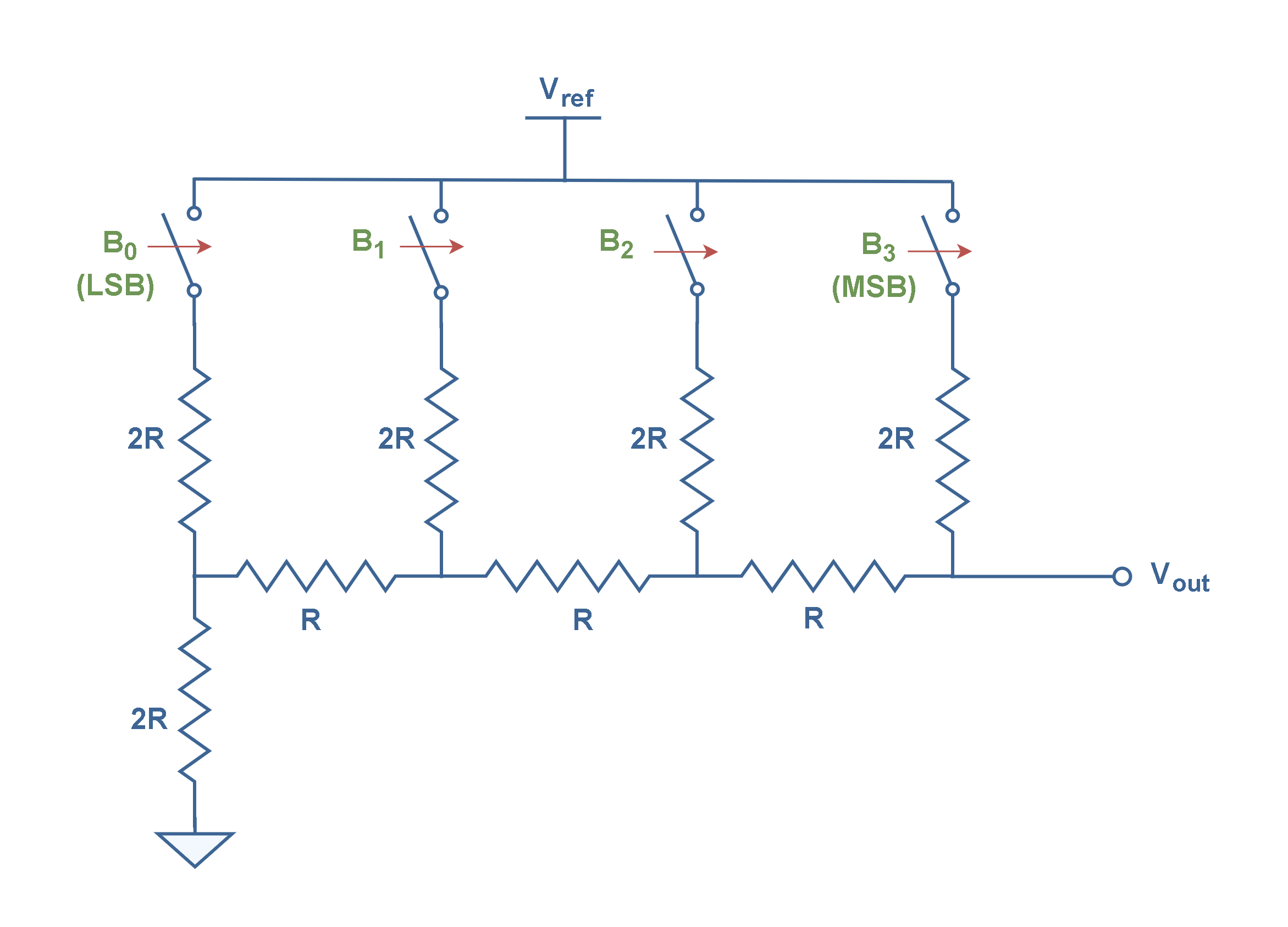
The “ladder” description comes from the ladder-like topology of the network. This configuration operates as an array of voltage dividers whose output accuracy is exclusively dependent on how well each resistor is matched to the others.
Note that the network consists of only two resistor values; R and 2R (twice the value of R) no matter how many bits make up the ladder. For this reason, the R/2R ladder is inexpensive and relatively easy to manufacture. All bits pass through resistance of 2R. The less weighty the bit, the more resistors the signal must pass through before reaching the output.
The digital inputs or bits range from LSB (B0) to MSB (B3). The bits are switched between 0 Volt and Vref and each binary input adds its own weighted contribution to the analog output Vout depending on the state and position of the bit. The MSB causes the greatest effect in output voltage and the LSB causes the smallest.
By methodical application of Thevenin’s Equivalent circuits and Superposition Principle, it is possible to analyze the R-2R circuit. With the help of simple mathematics, it can be proved that the analog output voltage Vout in the case of binary ladder network of Figure 5 is given by Equation 8.
This configuration is easily extendable. Equation 9 explains how to calculate the analog output voltage Vout for a ladder network with n bits.
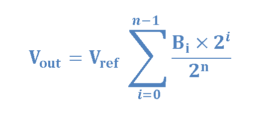
Figure 6 shows a more practical implementation of the R/2R resistor ladder network as a digital-to-analog converter using an op-amp as an inverting summing amplifier.
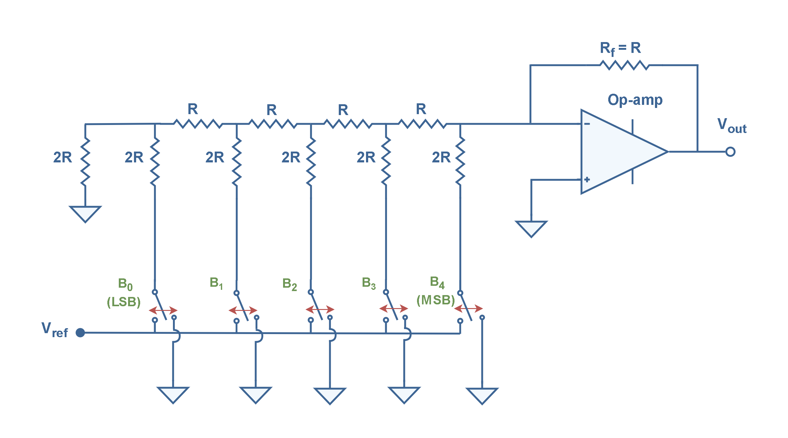
This type of DAC is also known as a multiplying converter. The output voltage is linearly proportional to the digital input states and the range can be adjusted by changing the reference voltage Vref. The Thevenin resistance of an R/2R ladder is always R –regardless of the number of bits in the ladder. Therefore, in this configuration, the source impedance as seen by the op-amp is always constant and equal to R.
The output voltage is the result of Equation 10.
A binary ladder R/2R network is the most widely used network for digital-to-analog conversion for obvious reasons:
- Easily scalable to any desired number of bits
- Uses only two values of resistors which makes for easy and accurate fabrication and integration
- Having a fixed output impedance of the ladder (R) simplifies filtering and further analog signal processing and circuit design
- The R/2R network provides an accurate method of digital-to-analog conversion.
Such D/A converters of different sizes (eight-bit, 12-bit, 16-bit, etc.) are available in the form of monolithic integrated circuits.
Summary
- A digital-to-analog converter (DAC) takes digital data at its input and converts them into analog voltage or current that is proportional to the weighted sum of digital inputs.
- Digital codes are typically converted to analog voltages by assigning a voltage weight to each bit in the digital code. This function can be done by a simple resistive network.
- By summing the voltage weights of the entire code, the analog voltage is reconstructed.
- The most popular networks are the binary-weighted resistive and the R/2R ladder.
- Both circuits will convert digital voltage information to analog, but the R/2R ladder has become the most popular due to the network’s inherent accuracy superiority, and ease of manufacture.
- The R/2R ladder is made up of only two different values of the resistor. This overcomes one of the drawbacks of using precision resistors in the weighted resistive network.
- The R/2R ladder networks provide a simple, inexpensive way to perform digital-to-analog conversion.


