Bode Diagrams
Introduction It is in the late 30's that an American engineer named Hendrick Wade Bode designs a famous representation to study AC circuits in the frequency domain. These graphs are still nowadays very useful in electronics and automatism and are called Bode diagrams.
Introduction
It is in the late 30’s that an American engineer named Hendrick Wade Bode designs a famous representation to study AC circuits in the frequency domain. These graphs are still nowadays very useful in electronics and automatism and are called Bode diagrams.
In this tutorial, we will give every necessary step in order to represent and read Bode diagrams.
First of all, we present every necessary concept that needs to be detailed previously. We will, therefore, give a recap about the notions of the transfer function, gain, and phase.
The following of the article consists of understanding how to read these diagrams, which provides much information about an unknown circuit.
The last section shows how to plot the diagrams of some of the most common electronic circuits. This process is useful to share the information in a compact form of a specific circuit in a manual user for example.
Definitions
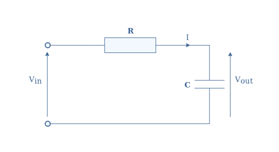
The transfer function is the fundamental notion to understand before talking about Bode diagrams. Consider any linear electronic circuit defined by its transfer function T(jω) and represented in Figure 1 by a box, with one input and one output terminal:
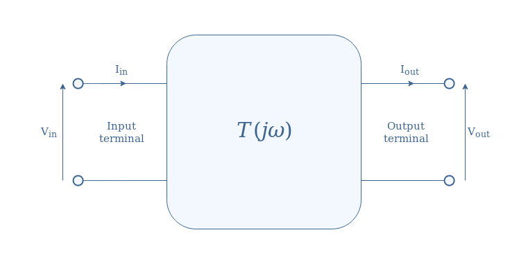
The transfer function is defined by Vout=T(jω)×Vin with Vin=|Vin|ejωt. Sometimes, we can note p or s=jω which is known as the Laplace variable.
From this transfer function, two important parameters can be computed. The first one is the gain/amplitude (G), which is found by taking the norm of this complex function: G=|T(jω)|. In order to plot Bode diagrams, it is the gain in decibels (GdB) that is considered: GdB=20log(G).
A gain GdB=0 indicates that the norms of the input and output are equal |Vin|=|Vout|, this is called a unitary gain. When GdB tends to infinite negative values, no output is observed despite the presence of an input.
The second important parameter is the phase difference (ΔΦ) between the input and output. This phase difference is given by the argument of the transfer function: arg(T(jω))=ΔΦ. This equality comes from the fact that if we consider a ratio of complex numbers z1/z2, the argument is given by the differences of the arguments of the numerator and denominator, which proves the previous formula: arg(z1/z2)=arg(z1)-arg(z2).
Presentation of Bode diagrams
The Bode diagram of an electronic circuit consists of two graphs that plot respectively the gain GdB and the phase difference as a function of the frequency in logarithmic scale. Both of these graphs can have two representations that are shown in Figure 2: the real or asymptotic representation.
The real curve is associated with the analytical expression of the norm and the argument of the transfer function. The asymptotic representation is a straight-line approximation also known as Bode pole. In this section, we study the Bode diagrams of a simple series RC low-pass filter which circuit is represented in the third section.
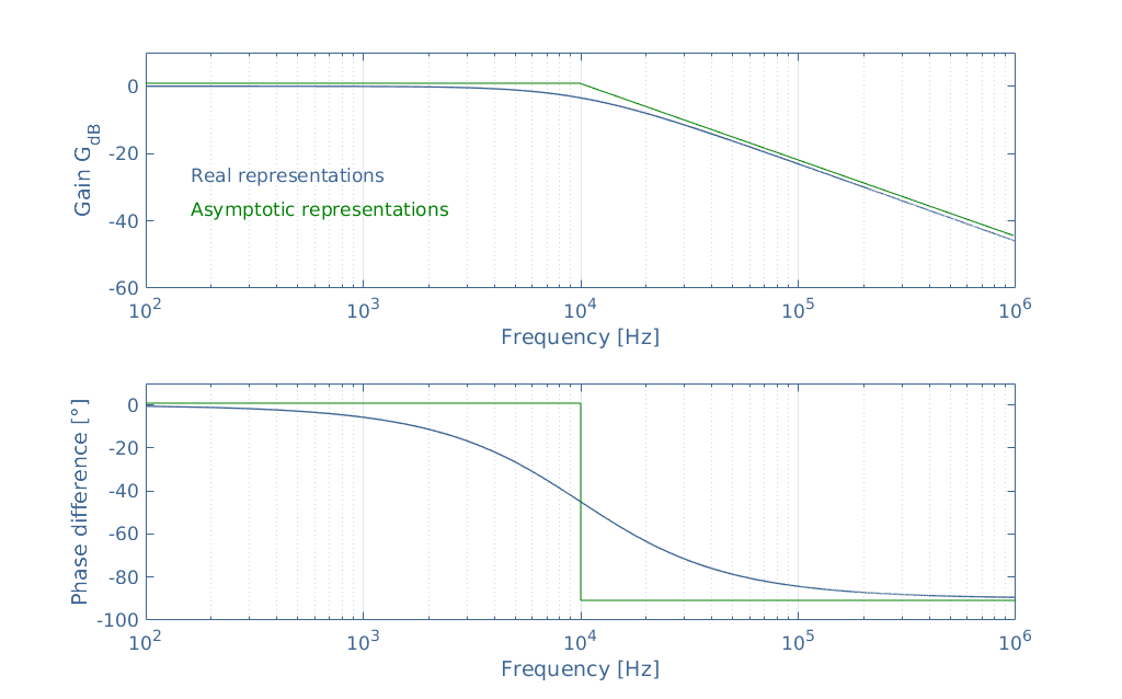
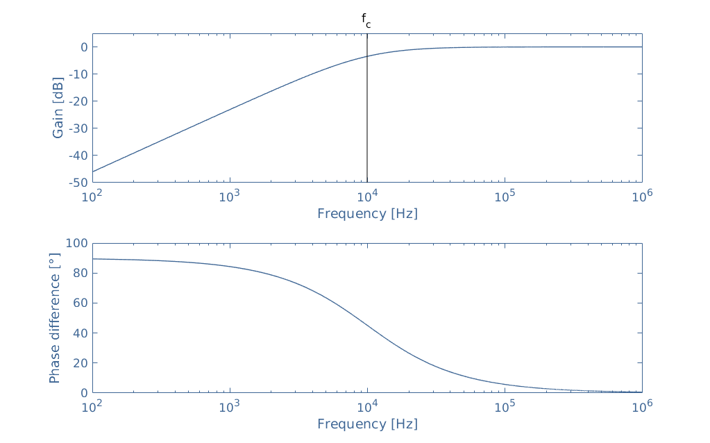
Figure 2 gives a lot of information, but in order to make it more clear and easy to read, we consider the real representations of the gain and phase plots separately in Figure 3 and Figure 4 as following.
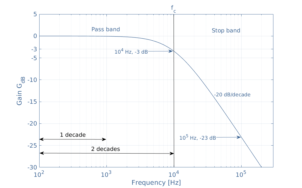
The gain plot is divided into two regions labeled pass band and stop band which common border is defined by the cutoff frequency fc and in this example is equal to 10 kHz. The pass band is the region where the gain is constant and equal to 0 dB (in the Bode pole approximation), the stop band is the region where the gain is strictly smaller than -3 dB and drastically decreases, this value and rate are commented more in detail in the following.
This specific frequency is characterized by GdB(fc)=-3 dB, but why is this value so relevant? Even if each circuit has different expressions for the transfer function and the cutoff frequency, the amplitude is always divided by √2 at fc: |T(fc)|=|Tmax|/√2. When converting this ratio in dB, it comes that 20log(1/√2)=-3.
The importance of this value comes from the fact that the power is proportional to the square of the amplitude, hence when the amplitude is divided by √2, the power is divided by 2.
One last fact can be commented in Figure 3, it is indeed highlighted that at 100 kHz the gain is -23 dB. Since at 10 kHz the gain is -3 dB, we observe a loss of -20 dB per decade, also written -20 dB/dec. We will see later in the third section that this value is typical from a first-order filter.
We can also extract some information from the phase plot shown in Figure 4 below:
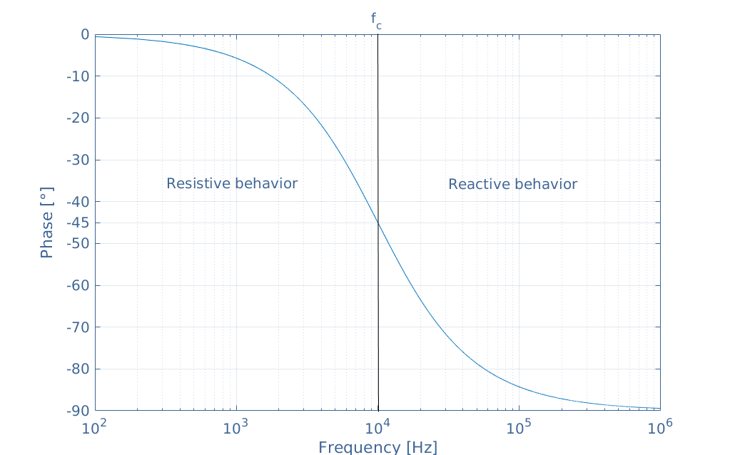
Here the same cutoff frequency marks the border between the resistive and reactive behavior. At fc, the phase-difference is indeed equal to -45°. Before fc, the circuit behaves more like a resistor, in DC and low-frequency regime, it is purely resistive. After fc, the capacitance effect increases and at high frequencies, the circuit becomes purely reactive.
Common Bode diagrams
First-order filters
The previous section presents the Bode diagram of a series RC low-pass filter which circuit is represented in Figure 5:
We have seen that this filter is characterized by its cutoff frequency fc=1/(2πRC), and it’s gain roll-off of -20 dB/dec. Let’s now consider another type of filter that can be realized with a parallel RC circuit shown in Figure 6:
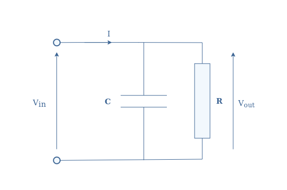
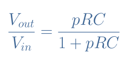
It can be shown that the transfer function of this circuit is given by Equation 1, with p=jω.
When plotting the Bode diagrams associated with this transfer function, it becomes clear that the parallel RC circuit is a high-pass filter:
For this example, we chose the same values of R and C than for the low-pass filter so that the cutoff frequency remains unchanged and equals 10 kHz.
Concerning the gain plot, we can say that it is the symmetrical plot of the low-pass filter with the vertical line given by the cutoff frequency value as the symmetrical axis. The pass and stop bands are inversed and a positive slope is now observed, which rate from the DC regime to the cutoff frequency is +20 dB/dec.
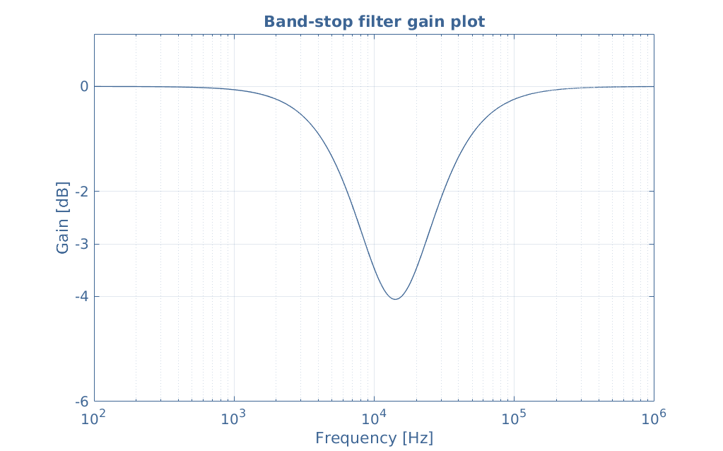
From the association of Bode diagrams, we can understand how band-pass and band-stop filters can be made. Consider indeed a low-pass and high-pass filters which cutoff frequencies are respectively fcl and fch. A band-stop filter behavior is observed if fcl<fch:
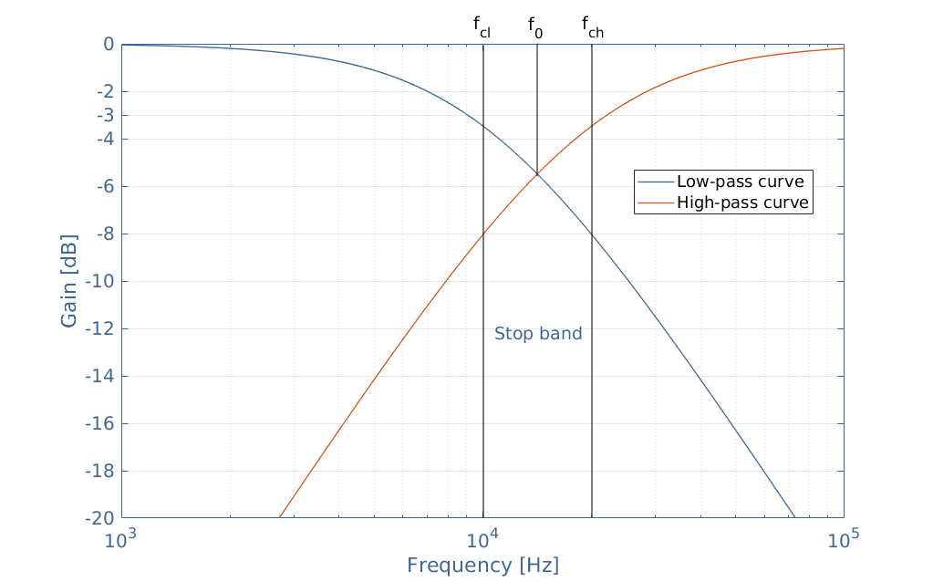
In this example, fcl=10 kHz and fch=20 kHz, the band-stop-width is therefore given by Δf=fch-fcl=10 kHz. The resonance frequency f0 is given by the geometrical mean of the cutoff frequencies: f0=√(fcl+fch)≈14 kHz. The gain plot of the band-stop filter is given by the logarithmic addition of these two curves:
A band-stop filter can be realized in practice by associating an RC high-pass filter in parallel with an RC low-pass filter and choosing appropriate values for the resistor and capacitor in order to observe the desired behavior.
The dual-circuit of the band-stop filter can be made with the series association of the same RC filters. In this case, the cutoff frequencies must respect the inequality fch<fcl:
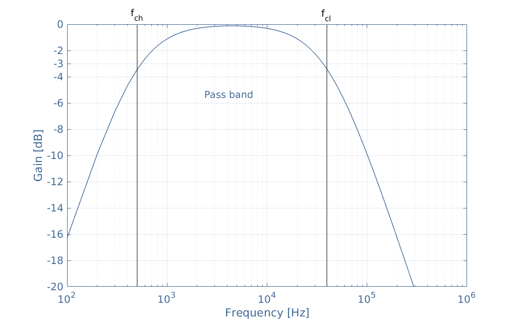
The formulas for the bandwidth and resonance frequency still apply for the band-pass filter.
Second-order filters
Second-order filters are characterized by the presence of at least one term p2 in the expression of their transfer function. This term comes from the fact that two reactive components are present in the circuit.
We have already presented in the Series RLC circuit and Parallel RLC circuit tutorials two circuits that respectively make second-order low-pass and high-pass filters. Their associated transfer function and Bode gain plots are also shown in these articles.
Second-order filters have the advantage of having a roll-off (for the low-pass filter) or an increase rate (for the high-pass filter) of 40 dB/dec in absolute value, therefore, rejecting faster the undesired frequencies.
Such as for first-order filters, second-order band-stop and band-pass filters can be realized with the parallel or series associations of the elementary RLC low-pass and high-pass filters.
Conclusion
Bode diagrams are a visual and efficient tool to represent the AC behavior of an electronic filter. They are associated with the transfer function of the circuit from which the gain and phase difference can be computed.
Bode diagrams can be plotted through some experimental methods in order to study and characterize an unknown circuit. The measure of the cutoff frequency, bandwidth (for band filters) and slope help us to determine the order, the components and the architecture of a circuit.
On the other hand, the knowledge of Bode diagrams of the elementary filters is essential to anticipate the behavior of a circuit and design customized filters.


