
Analog to Digital Converter (ADC)
- Muhammad Shahid
- m_shahid@live.co.uk
- 15 min
- 257 Views
- 0 Comments
- 0 Likes

Analog to Digital Converter
An analog-to-digital converter (ADC) is an electronic circuit that is used to convert a real-world signal into a digital or binary code. Real-world signals are usually taken from a sensory system which are generally analog in nature and represent instantaneous value of the measured entity. The sensory system may represent any real-world data such as temperature, pressure, light, sound, level, position, etc. In order to process, manipulate, or store these signals, it is feasible to convert them into a binary code or digital signal which is understandable by a microprocessor/ microcontroller unit. This process of conversion from analog (real-world) signals into a digital value is referred to as an Analog to Digital Conversion and the device or electronic circuity performing this action is called an Analog to Digital Converter.
The converted digital signal or binary comprises a number of bits and characterizes the “Resolution” of an analog-to-digital converter (ADC). A larger binary number or a high-resolution ADC can accommodate more converted values compared to a low-resolution ADC. For example, a 4-bit ADC has 16 (24) values from 0 to 15 for representing an analog signal. Whereas, an 8-bit ADC has 256 (28) values from 0 to 255 for representation.
Before proceeding further, it is essential to first understand the major difference of continuity between an analog and digital signal.
Analog and Digital Signals
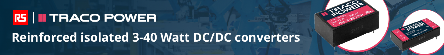
In the following figure, a potentiometer is used to select different voltage levels from 0 to VMAX depending on the position of the potentiometer’s knob. Whilst, moving through this range there is no obvious step or abrupt change in output voltage and finer values can be selected, carefully. In other words, it can be said that whilst moving from 0 to VMAX or any in-between positions of the potentiometer’s knob, the change in the output signal is continuous. This resembles analog signals generated by real-world sensors such as temperature, pressure, sound, and light intensity levels.
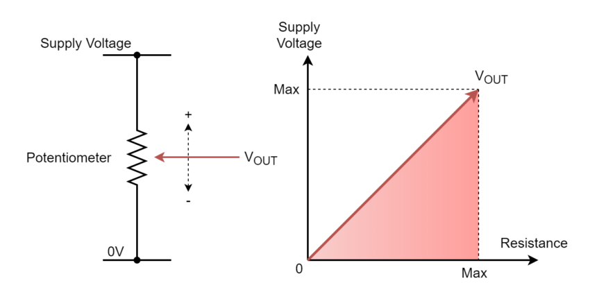
In contrast, the following figure shows different selectable positions of a rotary switch. Here, the range from 0 to VMAX, has been divided into different stages or levels which are selectable by rotary switch. Each stage comprises a resistor which is in series with preceding levels. This arrangement causes a voltage drop of a fixed level due to a fixed resistor at each level and as the resistors are also the same in values, therefore, each stage drops 1V. Hence, this kind of rotary switch has selectable voltage levels of 0V, 1V, 2V, 3V, 4V, and 5V. The output of such a rotary switch is discrete or non-continuous. Similarly, a “LOW” or a “HIGH” value, in the case of binary, is referred to as a digital signal as it represents discrete values.
Analog to Digital Converter
There are many ways to convert an analog signal into a digital equivalent and, as such, different electronic circuits can be constructed to achieve the conversion process. The easiest and more understandable ADC circuit can be constructed using discrete components such as multiple comparator converters or flash converters. In this, a number of comparator circuits are utilized to detect various voltage levels and are fed into an encoder. A comparison of an input signal is made against a reference voltage level to decide its voltage level or bin.
Comparator Circuit
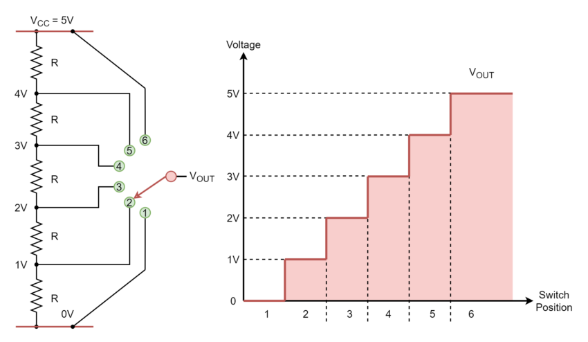
A single-bit comparator circuit can be constructed using an operational amplifier (op-am), such as LM339. An op-amp has two inputs: positive and negative and are used for comparing signals. An input signal (VIN) is applied on one pin whilst VREF is connected to the other pin. The comparison yields either “+V” or “0V” which can be translated into “HIGH” or “LOW”, respectively.
In case, an input (VIN) is less than (VREF) or (VIN < VREF) then the output is “LOW” and if an input (VIN) is greater than (VREF) or (VIN > VREF) then the output is “HIGH”. In the above figure, VREF is the output of a voltage divider circuit. As both resistors have the same value (ideally), therefore, voltage is divided into half (V/2) which is fed into the comparator as a VREF. So, an input signal in the voltage range of 0 to V/2 will yield an “0” output and an input signal’s voltage falling from V/2 to V gives a “1” output. So, a 1-bit is generated from such a comparator indicating the voltage category of an input signal. Generally, a (2n – 1) comparator would be required to generate a binary output comprising n-bits.
2-bit Analog to Digital Converter Circuit
In the following figure, a 2-bit DAC has been shown comprising of 3 comparators and that could be verified also using the formula (2n – 1) which gives a result of 3 for n = 2. In this circuit, four resistors of the same values are used that produce ideally equal voltage drops at the input of comparators. The input signal is compared by all comparators with these respective voltage drops.
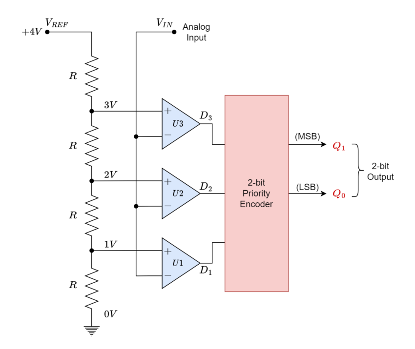
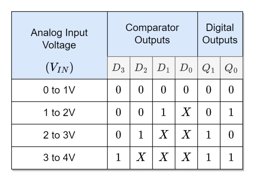
In order to ease the understanding process, VREF is kept at 4V so there is an ideally 1V drop across each of these four (04) resistors. So, when the input voltage is (0 < VIN <1V) then the output of all three comparators is zero i.e. D1 = D2 = D3 = 0, and the priority encoder outputs “00”. A priority encoder such as TTL 74LS148 uses priorities that are allocated to each input. In simple words, a priority encoder here converts or encodes three (03) inputs into a 2-bit digital number.
Likewise, continuing with the comparison process of the input signal, if the input voltage is (1 < VIN < 2V) then comparator (U1) will output a “HIGH” signal as, in this case, input voltage (VIN) is greater than the (VREF1 = 1V). The inputs at the priority encoder will be D1 = D2 = 0 and D3 = 1 which generates an output of “01”.
The same comparison procedure is followed for input voltages falling within ranges of 2 to 3V & 3 to 4V. The following table illustrates the input & output conditions of input voltage, comparator outputs, and digital outputs of the priority encoder.
The priority encoders are usually available commercially for 8-to-3-bit devices i.e. TTL 74LS148, whereas, in the above 2-bit ADC, a 4-to-2-bit priority encoder is used. A 4-to-2-bit priority encoder can be constructed using discrete components as shown in the following figure.
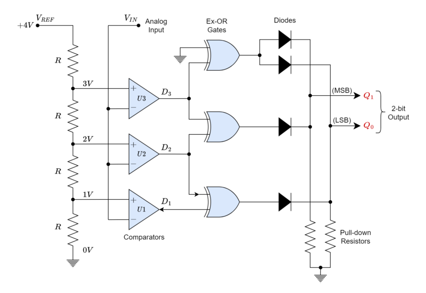
In the above circuit, Exclusive-OR (XOR) gates are used to generate output by comparing the outputs of adjacent comparators. In case, there are differentiating inputs i.e. “HIGH” and “LOW” or vice versa then XOR generates a “HIGH” signal and, a “LOW”, whenever both inputs are the same. The diodes are used to allow uni-directional flow of signal and pull-down resistors ensuring that none of the outputs floats to give erroneous digital outputs.
However, the resolution of this circuit is somewhat low i.e. 1V, and this can be improved by using higher resolution ADC such as a 3-bit ADC.
3-bit Analog to Digital Converter
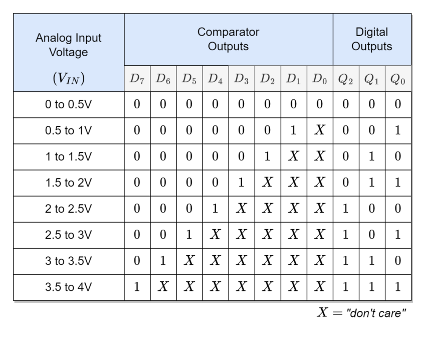
In a 3-bit ADC, a total of seven (07) comparators are required according to (2n – 1) using n = 3, and the voltage drop circuit will contain eight (08) resistors, accordingly. This means that stages of comparison have been increased from three (03) to seven (07) and the voltage comparison level has reduced from 1V to 0.5V (4V/8). So, this 3-bit ADC will be able to sense a change in voltage of 0.5V compared to 1V of a 2-bit ADC, consequently, yielding a high-resolution performance.
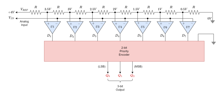
The following table depicts the comparator and digital outputs compared to input signal ranges for a 3-bit ADC.
Similarly, the construction of a 4-bit ADC requires 15 (24 – 1) comparators, and, likewise, 255 (28 – 1) & 1023 (210 – 1) comparators are required for 8-bit & 10-bit ADCs, respectively. So, with the increase in resolution, the circuitry becomes more and more complex. However, the parallel or flash-type analog to digital converters has the advantage of processing comparisons in parallel yielding a faster conversion result at its outputs.
Conclusion
- A digital-to-analog converter is an electronic circuit that interfaces with real-world signals and encodes them into a digital signal that is more suitable for data manipulation, storage, and transmission.
- The real-world signals generally represent physical quantities that are measured using different sensory systems such as temperature, pressure, electric & magnetic fields, sound & light intensity levels, etc. These real-world signals are analog signals that are continuous and contain infinite information.
- A digital signal is discrete in nature and has fixed steps or levels. Such as a binary signal has only zeros and ones or 0V & 5V in terms of voltage levels. The digital or binary signals are suitable for processing in digital systems with capabilities of manipulating, storing, and transmitting this digital data.
- A simple and widely used analog-to-digital converter is a flash or multiple comparators-based circuit that processes signal comparison in parallel using (2n – 1) comparators. Where “n” represents the number of digital output bits.
- The number of bits (n) defines the resolution of an ADC and a high-resolution ADC is more accurate in converting analog to digital signals because of the higher sensitivity to the magnitude of analog signal.
- The circuity of a flash or parallel comparator type ADC becomes more and more complex with the increase of resolution or number of output bits it produces. However, its conversion process is faster due to the simultaneous comparison of input signals across all comparators.
Please follow and like us:
Subscribe
Login
0 Comments


")