

Binary Adder
- Muhammad Shahid
- m_shahid@live.co.uk
- 586 Views
- 0 Comments
- 0 Likes

Binary Adder
A digital Binary Adder is a combinational logic circuit that performs the arithmetic operations of addition on binary numbers. The binary adders are usually classified into Binary Half-Adders or Full-adders which perform an arithmetic operation on two binary digits. A simple or basic Binary Adder can be constructed using Exclusive-OR (XOR) and AND Gates to add two binary numbers. As is the case with normal addition, an addition of two digits results in a SUM and a CARRY, and, in the case of binary digits, the addition yields a SUM bit and a CARRY bit.
In the following example, an addition is performed on two denary numbers. Each digit of a number, from least significant (rightmost) to most significant (leftmost), is characterized by a value depending on its power or position in the number.
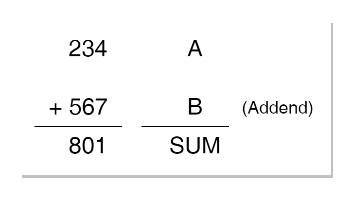
In the above addition, both numbers are added by adding digits belonging to the same column or power. The sum of digits would yield a value of either less than 10 or otherwise. In case the result of addition is less than 10 then only SUM, a single digit value of 9 or less, is written otherwise a carry (a value of 1) is added to the next high column addition.
Binary Addition
The Binary Addition follows the same procedure except for the addition of two binary digits cannot exceed a value of 2 i.e. 10 in binary. In the case of addition where binary digits sum exceeds “2” i.e. 1+1 then SUM = 1 & CARRY = 1 otherwise in the rest of the sum combinations (0+0, 0+1, and 1+0), a CARRY is not generated. The CARRY bit generated is then subsequently added to the next higher bit or column for addition. A similar method is followed for the next higher-order digits or columns. In the following figure, different addition combinations of single bits are illustrated to show SUM & CARRY bits.
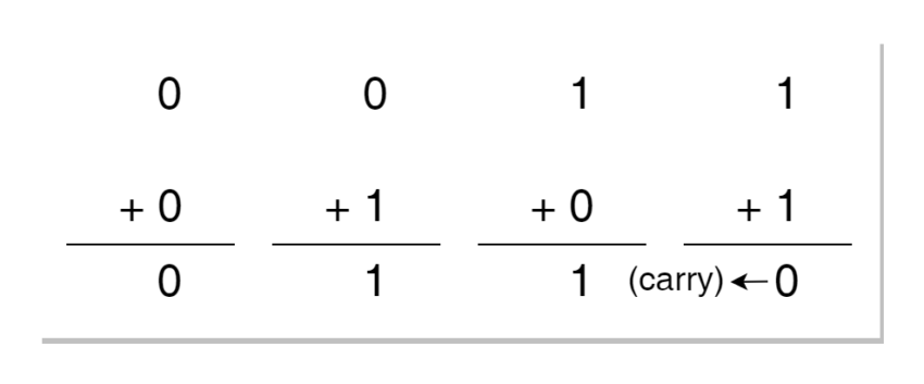
In the above figure, addition combinations of “0+0”, “0+1”, and “1+0” produce a SUM bit of “0” or “1”, however, a CARRY is always “0” and is only generated when there is a sum of “1+1”. This simple binary adder requires only two-bit inputs i.e. “A” & “B” and two-bit outputs i.e. SUM & CARRY.
This Binary Adder is termed a Half-Adder and can be represented through a simple block diagram given below:
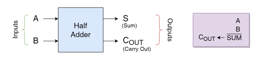
In Half Adder, the CARRY output generated can be ignored as there is no input to consider this CARRY generated from the preceding Half Adder. A careful observation of results produced on SUM output against different input combinations, yields that the outputs are similar to the one produced by an Exclusive-OR (XOR) gate. This can be illustrated if inputs of XOR Gate are labeled as “A” & “B” and single output as “S” to represent SUM. The following diagram of XOR Gate along with its Truth Table resembles the Half Adder output when CARRY output is ignored.
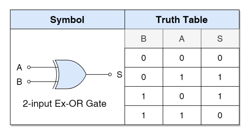
It is eminent from the above table that the “S” or “SUM” bit is produced (“1”) when there is an exclusive or different combination otherwise it is set to “0”. This means that the “SUM” output of a Half Adder can be generated using an Exclusive-OR (Gate). Whereas, the CARRY output is produced only when both inputs (A & B) are “HIGH” or “1” otherwise it is set to “LOW” or “0”. This desired function is analogous to the function of an AND Gate which is given below in the form of a Truth Table along with its symbol.
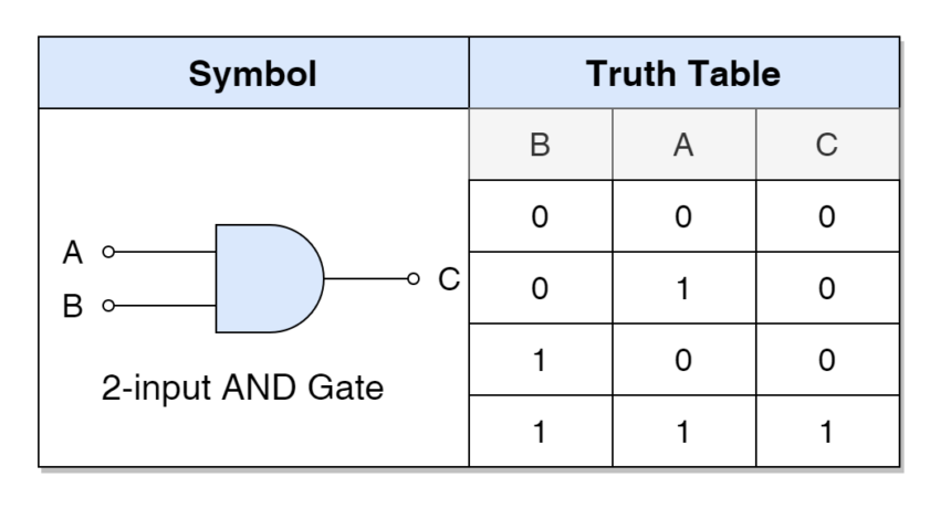
Hence, a Half Adder can be constructed using XOR and AND gates
Half Adder
It is a combinational logic circuit that performs the addition of two binary bits or digits which, consequently, produces SUM and CARRY binary digits (bits). The logic diagram of Half Adder with its Truth Table is shown below:
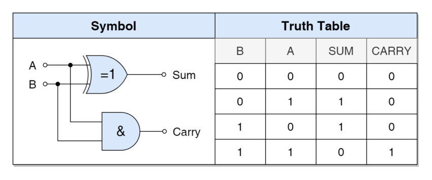
The SUM bit is an Exclusive-OR function which is given below:
SUM = A XOR B = A⊕B
Whereas, the CARRY bit is an AND function:
CARRY = A AND B = A.B
As discussed earlier, the Half Adder does not consider the input CARRY bit in its SUM function and, as such, cannot be used to cascade multiple Half Adders to perform SUM of binary numbers having more than one digit as the CARRY bit results from “1+1” cannot be passed to next higher bit addition. This can be regarded as one of the biggest disadvantages of a Half-Adder circuit. In order to overcome this disadvantage or perform the addition of more than one-digit binary numbers, a Full Adder circuit is utilized.
Full Adder
A Full Adder is another combinational logic circuit that performs an arithmetic operation of additions similar to the one performed by a Half Adder but, with the difference that a Full Adder considers CARRY at its input for performing the addition function. So, in addition to “A” & “B”, there is a “CIN” input that takes into account the carry-bit generated from the preceding sum operation. A Full Adder circuit is illustrated by the following diagram.
Figure 7: Full Adder Circuit and Truth Table
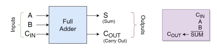
From the above figure, a Full Adder is a combination circuit that performs addition on three bits which includes a Carry-bit (Carry In) generated by the addition of less significant binary digits and two outputs including a Carry-bit (Carry Out) to be considered for addition in next more significant binary digits.
A Full Adder can be constructed using two Half Adder circuits where the second Half Adder sums the Carry input (CIN) and Sum (SUM) generated by the first Half Adder, as shown in the following logical diagram.
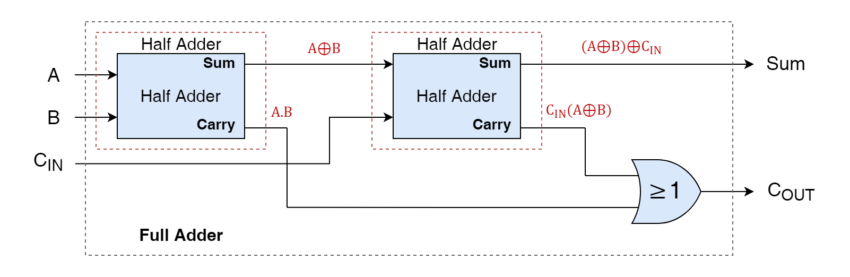
In the following figure, a basic logical diagram of a Full Adder with its Truth Table is given.
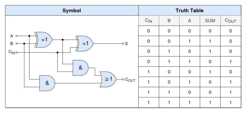
The Full Adder can also be represented by Boolean Algebraic expressions for SUM and CARRY-OUT bits:
For SUM bit:
SUM=(A XOR B) XOR Cin = (A⊕B)⊕Cin
For CARRY-OUT:
CARRY-OUT = A AND B OR Cin(A XOR B) = A.B + Cin(A⊕B)
n-bit Binary Adder
The addition of single binary digits or bits can be performed using a Half Adder circuit described above and for the addition of binary numbers having more than one binary digit, Full Adder circuits in cascade arrangement are used. Such arrangement of Fuller Adders is commonly known as Ripple Carry Adder as the transportation of carry bit from one full adder to other significant ones resembles a Ripples effect.
In the following diagram, a Ripple Carry Adder example has been shown to add 4-bit binary numbers. In this diagram, each Full Adder represents the addition of a weighted column and produces two outputs i.e. “SUM” and “CARRY OUT” which are then fed into the next significant column or Full Adder. The process repeats until the CARRY OUT reaches the most significant column or Full Adder. This passing of CARRY OUT from least significant to most significant resembles the Ripple Effect.
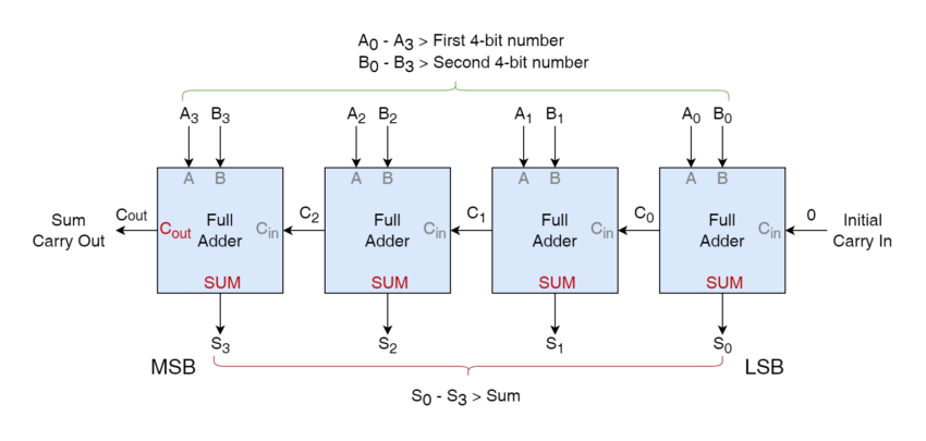
In the Ripple Carry Adder discussed above, the Carry Bit is transmitted from least significant to most significant column addition in steps and each Full Adder takes require some time to respond to its inputs to produce outputs. This response time in logic gates is referred to as “Propagation Delay” and cascaded of Full Adders for adding binary numbers increases this “Propagation Delay”. The outputs of the most significant Full Adder are delayed depending on the numbers of preceding Full Adders. This could lead to a serious problem when binary numbers being added are large i.e. 32 or 64 bits or the system requires a high clock speed. This can be regarded as one of the disadvantages of a Ripple Carry Adder.
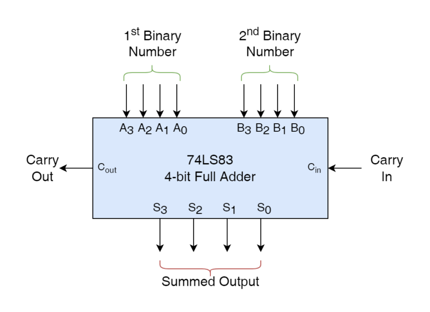
A Carry Look Ahead Binary Adder significantly reduces the operation time by generating carry input signals directly from the inputs which makes it independent of the number of bits used in addition. The Carry Look Ahead Binary Adder circuits are commercially available in TTL binary adders, such as 74LS83, 74LS283, and CMOS 4008 which enable the addition of 4-bit binary numbers. In the following figure, a TTL 74LS83 package with pinouts has been shown.
Conclusion
- A Binary Adder is a combinational logic circuit that performs the addition of Binary Numbers. The addition of Binary Numbers is similar to the method used for the addition of denary numbers except, in Binary Numbers, a Carry is generated when a sum is equal or greater to “2”.
- A basic Binary Adder adds two single binary digits or bits producing a “SUM” and a “CARRY OUT” bit and is called Half Adder. A Half Adder circuit ignores “CARRY IN” generated from preceding less significant addition and, as such, is unsuitable for the addition of multi-bit binary numbers.
- A Full Adder considers the “CARRY IN” in performing the addition function and can be cascaded with other Full Adders to perform the addition of larger binary numbers but this cascaded arrangement is prone to “Propagation Delay”.
- A cascaded arrangement of Full Adders is termed as Ripple Carry Adder because the transportation of Carry Bit from least significant to most significant Full Adder resembles the effect of Ripple.
- The Carry Look Ahead Binary Adder directly takes into account the binary inputs to generate Carry Bit rather than delaying for cycle time required to complete the SUM operation of a Full Adder and is independent of the number of bits used in addition.
- The 4-bit Carry Look Ahead Binary Adders are available in commercial IC Packages i.e. TTL 74LS83, 74LS283, and CMOS 4008.
Please follow and like us:
Subscribe
Login
0 Comments


")
