Engineer Designs a Computer in One Week With Quilter’s “Physics-Driven” AI
Project Speedrun’s AI-designed computer was built around the NXP i.MX 8M Mini processor and achieved first-boot success within a week, demonstrating autonomous PCB design.
The long-held standard for high-complexity PCB design, a multi-month cycle requiring extensive manual placement, routing, and iterative respins, has been challenged by new physics-driven AI technology.
Quilter, a developer of AI tools for electronics design, recently completed “Project Speedrun,” demonstrating the fully autonomous layout of a functional embedded computer in under one week. The initiative successfully compressed a workflow that conventionally spans multiple quarters for an entire engineering team into rapid weekly experiments.
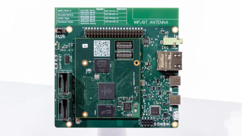
An engineer using Quilter’s AI was able to design a computer in under a week. Image used courtesy of Quilter
Quilter’s Project Speedrun
The computer design at the core of Quilter’s Project Speedrun is a two-board System-on-Module (SOM) and baseboard architecture based on the widely used NXP i.MX 8M Mini processor (Quad Cortex-A53 at 1.8 GHz). This platform, commonly found in embedded systems such as automotive infotainment and machine vision, necessitated a complex board design comprising 843 components and 5,141 total pins.
The final fabrication-ready design utilized an eight-layer high-density interconnect stack-up. Technical specifications for the layout included a 2 mil trace/space geometry for the SOM and 3.5 mil for the baseboard, indicative of production-grade precision requirements. The system’s memory specifications include 2 GB LPDDR4 with a 32-bit bus width, 32 GB eMMC 5.1, and 32 MB QSPI NOR Flash. Connectivity provisions include 10/100/1000 Mbps Ethernet and an M.2 connector supporting PCIe expansion.
Crucially, the completed hardware was reported to be fully functional upon first power-up. Achieving first-pass success on a complex embedded system of this density and architecture is a rare outcome in traditional PCB development, which typically budgets for multiple design respins to resolve integration and signal integrity issues.
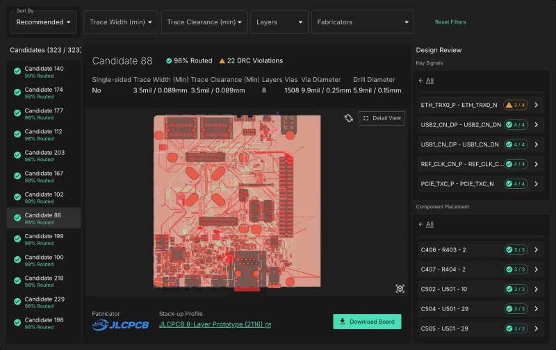
Project Speedrun’s AI runtime involved 27 hours of placement, routing, and validation. Image used courtesy of Quilter
Autonomous Placement and Routing Metrics
The efficiency gains reported by Project Speedrun are primarily attributed to the deployment of Quilter AI, which uses physics-driven reinforcement learning to explore manufacturable board layouts. Instead of operating as a copilot or traditional autorouter, the system autonomously handles component placement, signal routing, and physics validation based on the engineer’s schematic and defined constraints.
Quilter provided quantitative comparative data detailing the labor reduction for the project. Professional PCB designers estimated the manual creation of the two-board system would require 428 hours of engineering time (238 hours for the baseboard and 190 hours for the SOM).
In the AI-assisted process, the Quilter engine completed 98% of the placement, routing, and initial physics validation autonomously in 27 hours. A single engineer was then required to perform 38.5 hours of cleanup, focusing on elements like PDN pours, via clusters, and minor footprint swaps, without needing significant signal trace rip-ups or design corrections. This input broke down to 12 hours for the baseboard and 26.5 hours for the SOM.
The resulting 38.5 hours of total human labor to reach a fabrication-ready state represents an approximately 11x acceleration compared to the estimated 428 hours of manual effort. The system’s ability to parallelize design exploration and embed continuous physics checks during the layout process eliminated traditional bottlenecks associated with signal integrity and manufacturability validation, directly enabling the first-pass functional success.
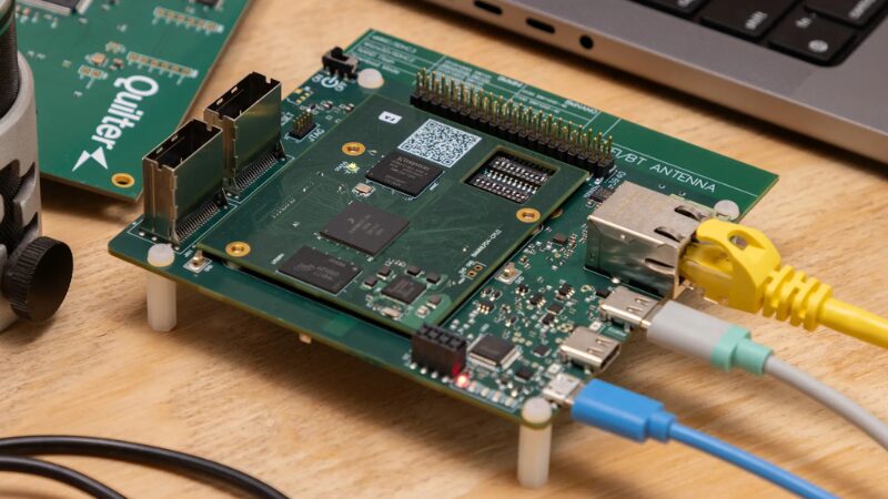
Quilter hopes that by compressing design time into weeks, rather than months, engineers will be able to shift their time to higher-value tasks. Image used courtesy of Quilter
Accelerating PCB Design
Project Speedrun has validated a methodology for generating complex, high-density PCBs using physics-driven AI, moving the design process from a sequential, iteration-heavy workflow to an autonomous, constraint-based one. The 11x acceleration and avoidance of design respins suggest a substantial shift in the hardware development pipeline.
For electrical engineers, this capability allows for a rapid prototyping and iteration cycle, moving high-complexity boards like those used in aerospace, medical devices, automotive systems, and advanced consumer electronics from schematic capture to fabrication in days, rather than months.


