Positive Feedback in Electronic Circuits
Introduction While negative feedback controls and corrects the behavior of a system, positive feedback encourages and strengthens the behavior of the system. For this reason, it is also known as regenerative feedback.
Introduction
While negative feedback controls and corrects the behavior of a system, positive feedback encourages and strengthens the behavior of the system. For this reason, it is also known as regenerative feedback. Positive feedback generally occurs when the fed-back signal is in phase with the input signal, and it causes the magnitude of the input signal to be increased, i.e., it improves the overall gain of the system.
Figure 1 shows the difference between mechanisms of feeding output signal to the input terminal in the case of in-phase (positive feedback) and 180° phase-shifted (negative feedback) feeding signal. The main 2-port linear network, like an amplifier, has an open-loop gain of ‘A’, and the feedback network has the transfer function with the magnitude of ‘β’. Obviously, the feedback signal comes to the input terminal after a small delay time, and then it is combined with the input signal, which is sketched here as a sinusoidal waveform.
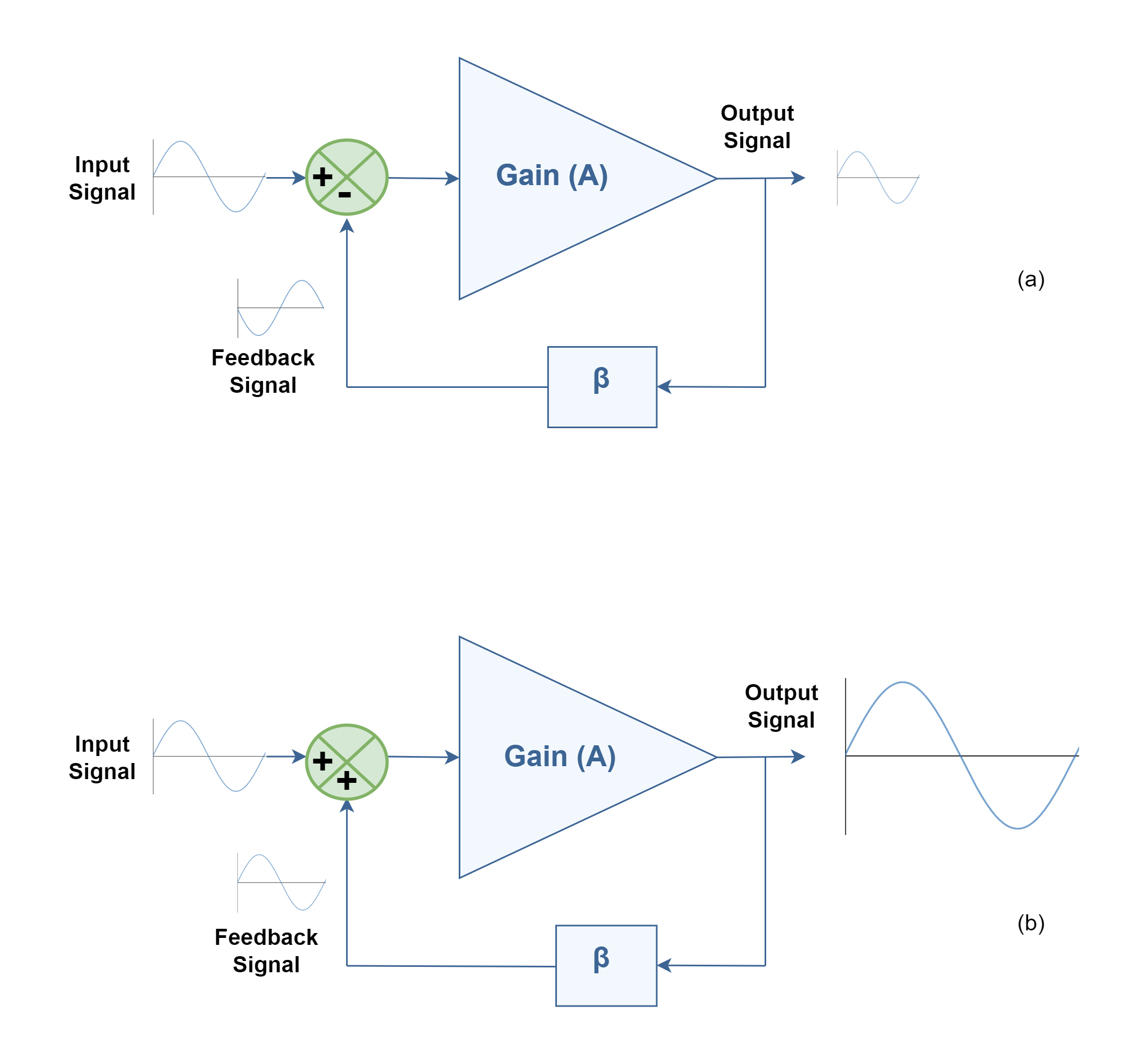
Figure 1: Comparison of 2 types of feedback configurations containing negative feedback (a) and positive feedback (b)
A key feature of positive feedback is that small disturbances get bigger. When a change occurs in a system, positive feedback causes further change, in the same direction until the output gets as high as it can go. Under certain gain conditions, positive feedback reinforces the input signal to the point where the output of the device oscillates between its maximum and minimum possible states (upper- and lower- rails). Therefore, the amount of positive feedback allowed is typically very limited to cause only small changes to the input signal.
In practical domains, while negative feedback is often used to create controlled amplifiers and filters, positive feedback is seldom used in amplifiers, since it normally increases distortion and instability. However, the positive feedback mechanism is employed in oscillator circuits.
It should be noticed that there are also certain conditions in which positive feedback is not good for semiconductor junctions and can harm them by thermal runaway.
Positive Feedback In Op-amps
With positive feedback in Op-amp amplifiers, the feedback voltage to the noninverting input will drive the op-amp harder in the direction of the output generated signal i.e., toward saturation. Figure 2 shows the simplest schematic circuit of an op-amp positive feedback configuration by connecting directly the output terminal (Vout) to the noninverting input terminal (V+). In this arrangement, the external input voltage source (Vs) can be inserted at the inverting terminal (V–). Two positive and negative DC power supplies provide biasing of the op-amp.
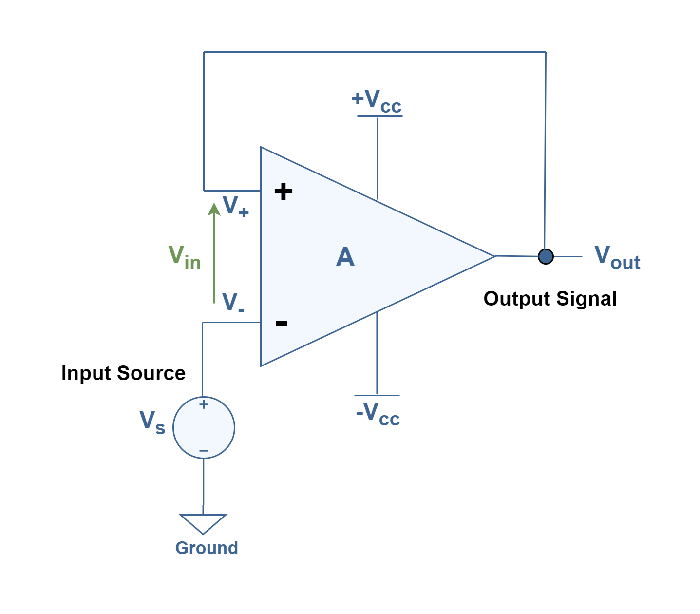
Figure 2: An op-amp circuit with simple positive feedback
If the inverting input is grounded (maintaining V– terminal at zero volts by removing the input voltage source of Vs), the output voltage will be manipulated just by the magnitude and polarity of the voltage at the non-inverting input (V+). If this voltage happens to be positive, the op-amp will drive its output positive as well. Feeding that positive voltage back again to the noninverting input will result in positive output saturation which is equal to the positive power supply voltage of Vcc i.e., the upper rail. Thus:
- Case 1: if V– = 0 and V+ > 0 then Vout = +Vcc
On the other hand, if the voltage on the noninverting input happens to become negative, the op-amp’s output will drive in the negative direction, feeding back to the noninverting input and resulting in full negative saturation (-Vcc or the lower rail). So:
- Case 2: if V– = 0 and V+ < 0 then Vout = -Vcc
This simple analysis can be completed by applying input external excitation (Vs) and changing the voltage at inverting terminal (V–) and obtaining the same results. Therefore, what we have here is a circuit whose output is bistable; it means being stable in one of two states (saturated positive or saturated negative). Once it has reached one of those saturated states, it will tend to remain unchanged or latch in that state. By placing a voltage upon the inverting (V–) input with the same polarity, but with a slightly greater magnitude, the present state will be switched to the next.
Positive Feedback Using Resistors
It is possible to have better control of the performance of this feedback system by adding 2 resistors between the input and the output terminals in the path of feedback. Figure 3 illustrates such a configuration by adding Rf and Rin to the op-amp and inserting an input voltage source (Vs) at the noninverting terminal (V+) while the inverting terminal (V–) is grounded.
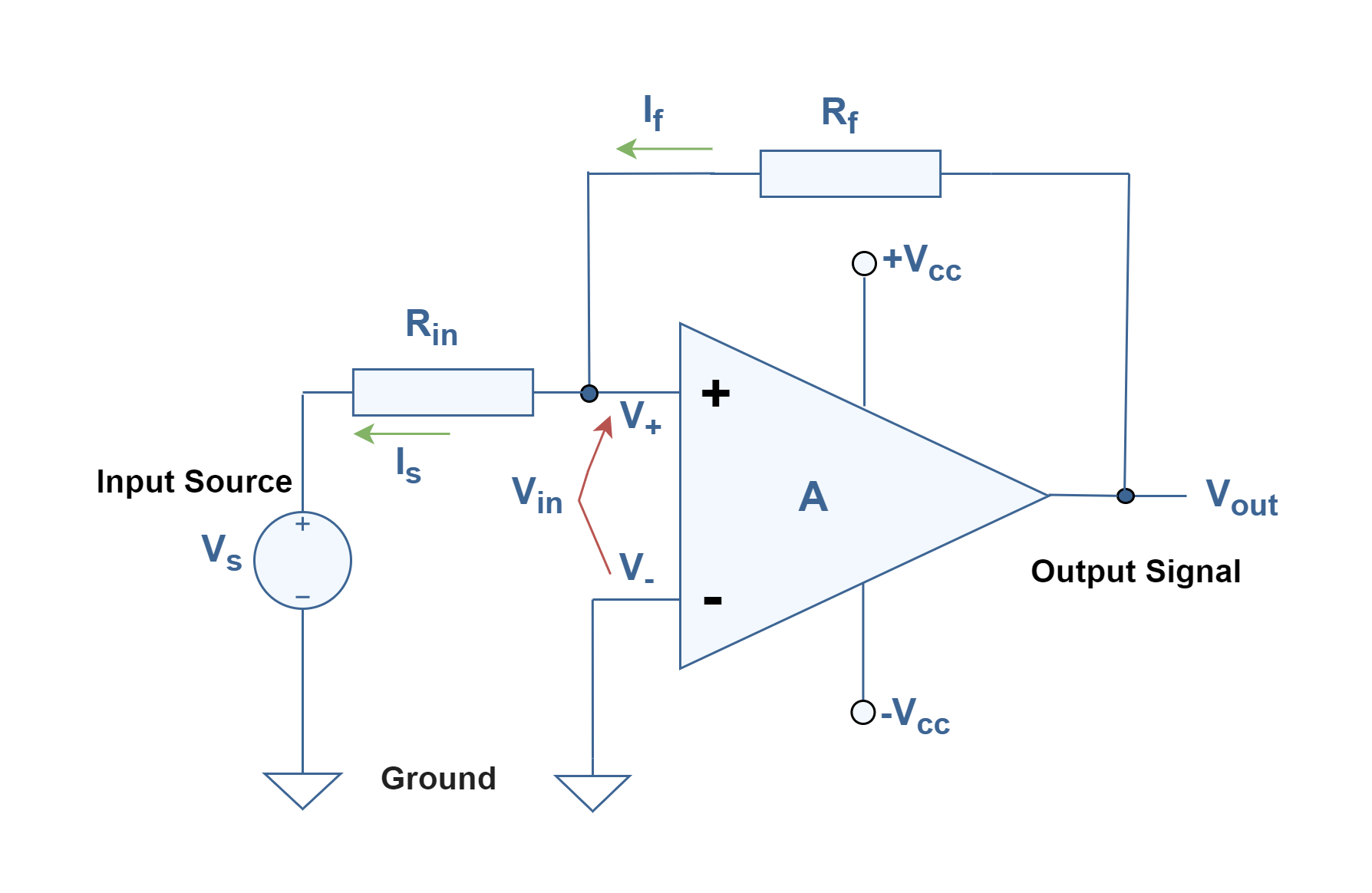
Figure 3: Configuration of a positive feedback op-amp circuit as a comparator
A Digital Comparator Using Positive Feedback
One application of this circuit is a digital comparator, to convert a continuous analog signal to a two-state discrete signal. Also, by adjusting the size of the feedback resistor, a comparator can be made to experience what is called hysteresis. In effect, hysteresis gives the comparator two thresholds. By obtaining these thresholds, the comparator circuit becomes more immune to noise voltages that can produce unwanted swings in the output. The hysteresis causes the output to remain in its current state unless the input voltage undergoes a major change in magnitude.
Figure 4 displays the amplitude waveforms of the input signal (Vin) and the output signal (Vout) versus time.
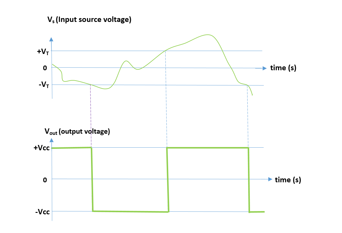
Figure 4: Waveforms of the input signal (Vs) and the output signal (Vout) versus time
Vin is defined as the difference between noninverting and inverting voltages while:
Vin = V+ – V–
To analyze the operation of the system we can first assume that the op-amp’s output is at positive saturation (+Vcc). Since V– is grounded, it is equal to 0 V. Because of the high impedance input characteristic of the op-amp, there is not any current inside the op-amp and the main current goes just through resistors of Rf and Rin. So, the two currents are equal; If = Is.
Using Ohm’s law:
If = (Vout – Vs) / (Rf + Rin)
By using the superposition principle, we first assume that Vs = 0, i.e., Rin is grounded. So:
Vin = Rin . If
The output remains at positive saturation (+Vcc). Now we assume that Vs has a non-zero value. If Vs is gradually reduced, there will be a point when Vin goes to 0 V, and the state of the output will be switched to another state (-Vcc). This voltage is called the negative threshold voltage (Vs = -VT) at the input. The negative threshold voltage can be determined by using the previous equations:
If = -VT / Rin = Vout / Rf = -Vcc / Rf
and then,
VT = Vcc (Rin / Rf).
Therefore, the width of the hysteresis region can be controlled by the ratio of the input and the feedback resistors. Now, if the output is at negative saturation (-Vcc) and 0 V is applied to the input (Vs = 0), Vin becomes negative and the output remains at (-Vcc). However, if the input voltage (Vs) is non-zero and it becomes increased, there is a point where Vin goes to zero, and the output switches states. This point is called the positive threshold voltage (Vs = +VT), which is equal to +Vcc. (Rin/Rf). In most applications, Rf is much larger than Rin.
Figure 5 shows the relationship between the output saturation voltages and the margin of threshold voltages at the input. Arrows show the possible paths of changing the output voltage due to changes in the input source of voltage.
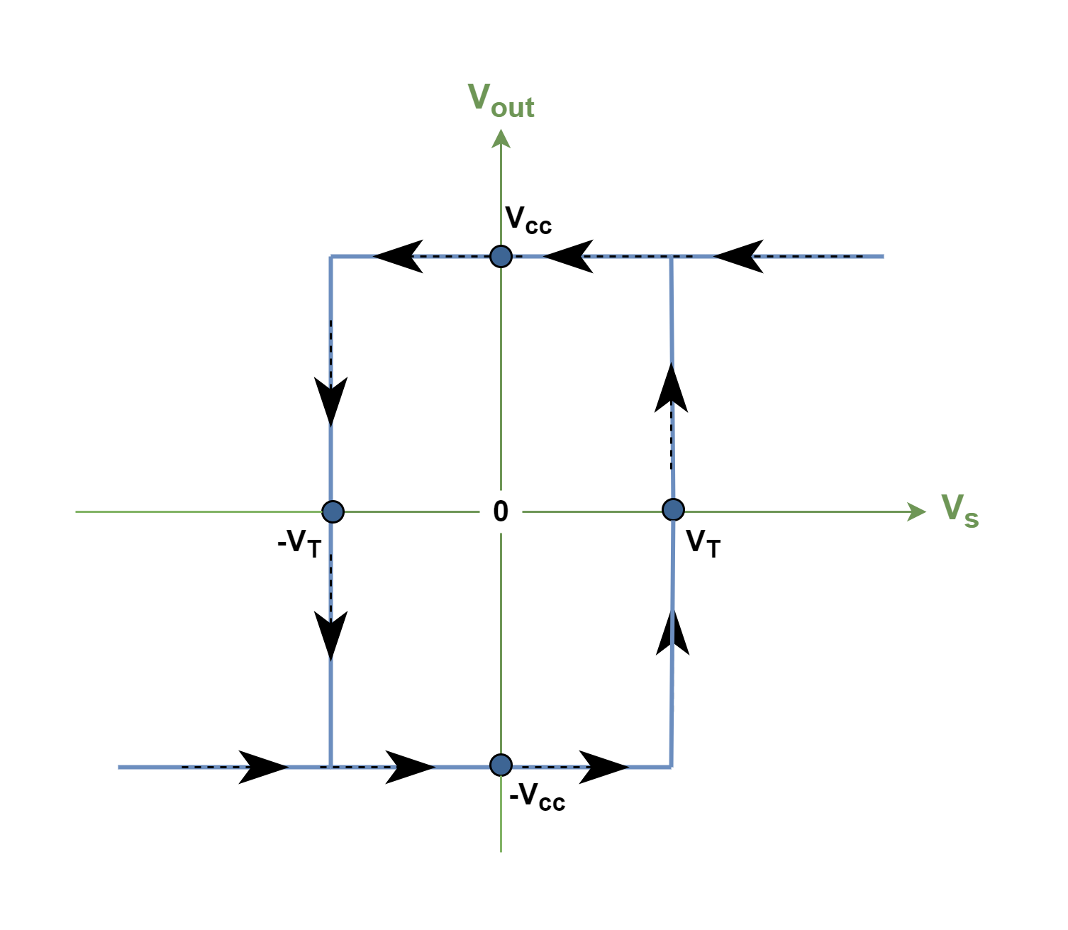
Figure 5: Hysteresis and threshold voltages in positive-feedback comparator
As Figure 4 shows clearly, applying a little positive feedback to the comparator and introducing threshold margins cause to extract of a clean square wave in the output, despite significant amounts of distortion and unwanted swings in the input signal.
Oscillation In Networks with Positive Feedback
The advantages of feedback, however, are accompanied by corresponding disadvantages. Since the magnitude and phase of the gain of each network vary with frequency, it is probable in certain conditions to introduce sufficient phase-shift to cause positive feedback. Under these circumstances, the amplifier may become unstable and generate an output signal independent of the input (or without input signal); in other words, it oscillates unexpectedly.
The oscillation occurrence is mostly harmful in amplifier circuits and it is a disadvantage. But in applications like communication systems oscillators are advantageous and widely used in modulation circuits and timing applications.
For better understanding, it is important to notice the denominator in the basic negative feedback equation, Af = A/ (1 + βA). When βA= –1 or a magnitude of 1 at a phase angle of 180°, the denominator becomes 0, and the gain with feedback ‘Af’ mathematically becomes infinite or very high physically. Thus, a very small signal (like a noise voltage) can provide a measurable output voltage, and the circuit acts as an oscillator even without an input excitation.
Figure 6 shows block diagrams of a general feedback system. If there is a fictitious voltage at the amplifier input ‘Vin’, it results in an output voltage of Vout = AVin after the amplifier stage and in a voltage Vf = β(AVin) after the feedback stage. Where βA is referred to as the loop gain.
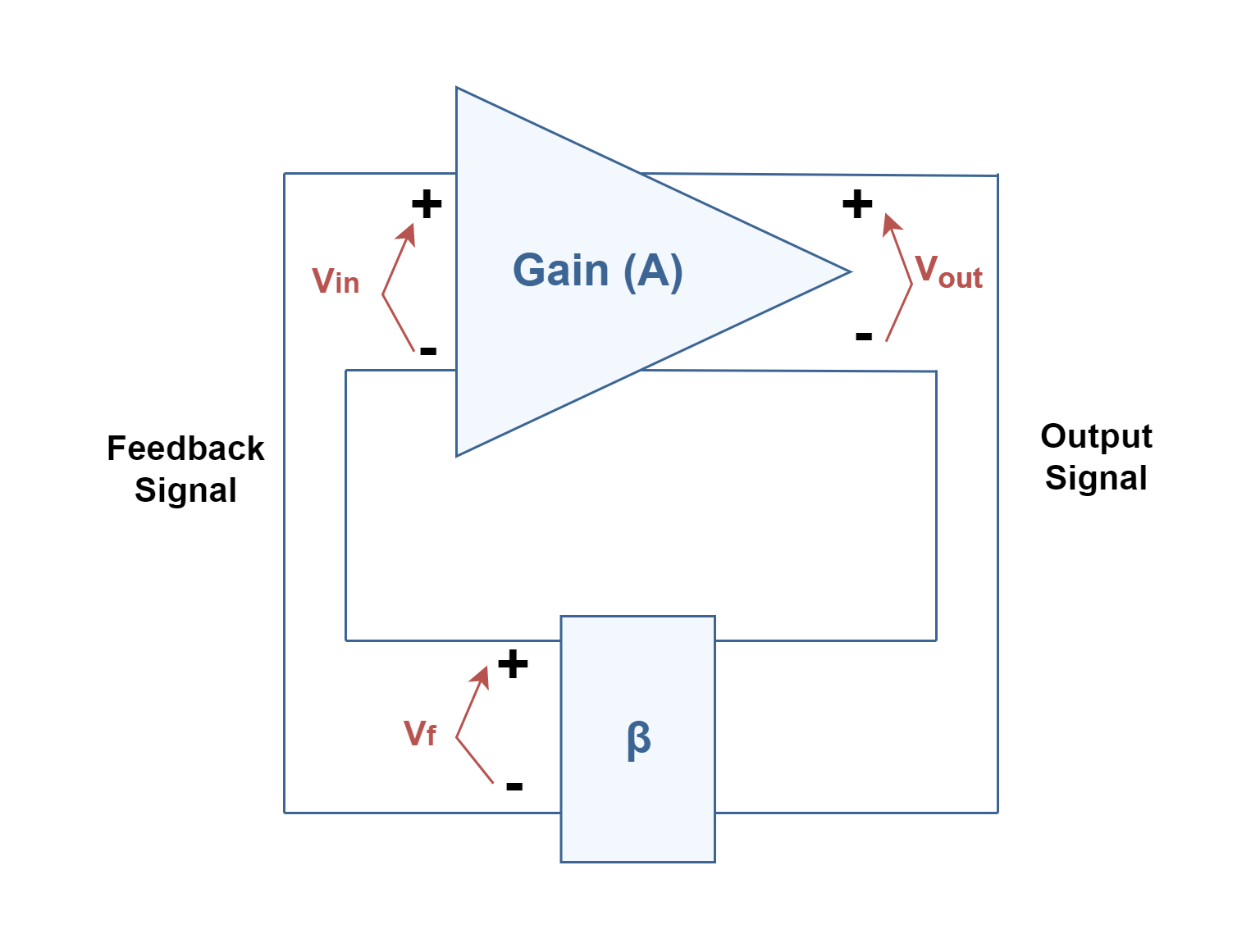
Figure 6: A general feedback system without external excitation
If the circuits of the base amplifier and feedback network provide βA of a correct magnitude and phase, Vf can be produced equal to Vin. Then, when even the fictitious voltage Vin is removed, the circuit will continue operating since the feedback voltage is sufficient to drive the amplifier and feedback circuits. Therefore, the output waveform will still exist even without any input excitation, if the condition βA = 1 is met. This is known as the Barkhausen criterion for oscillation.
In practice, no input signal is needed to start the oscillator going. Only βA is made equal to or greater than 1 and the system is started oscillating by amplifying noise voltage, which is always present. Such oscillations are sometimes called parasitic oscillations.
Figure 7 shows how the noise signal results in a buildup of a steady-state oscillation condition. In this waveform, three-section can be recognized: (a) In this period of time certain conditions are provided for an initial noise voltage to be amplified and appear at the output. (b) In the next period of time, this small non-sinusoidal signal (because βA is not perfectly 1) will be progressively gained in magnitude due to the positive feedback procedure. (c) the output waveform reaches a steady-state oscillation with a limited envelope due to circuit saturation conditions.
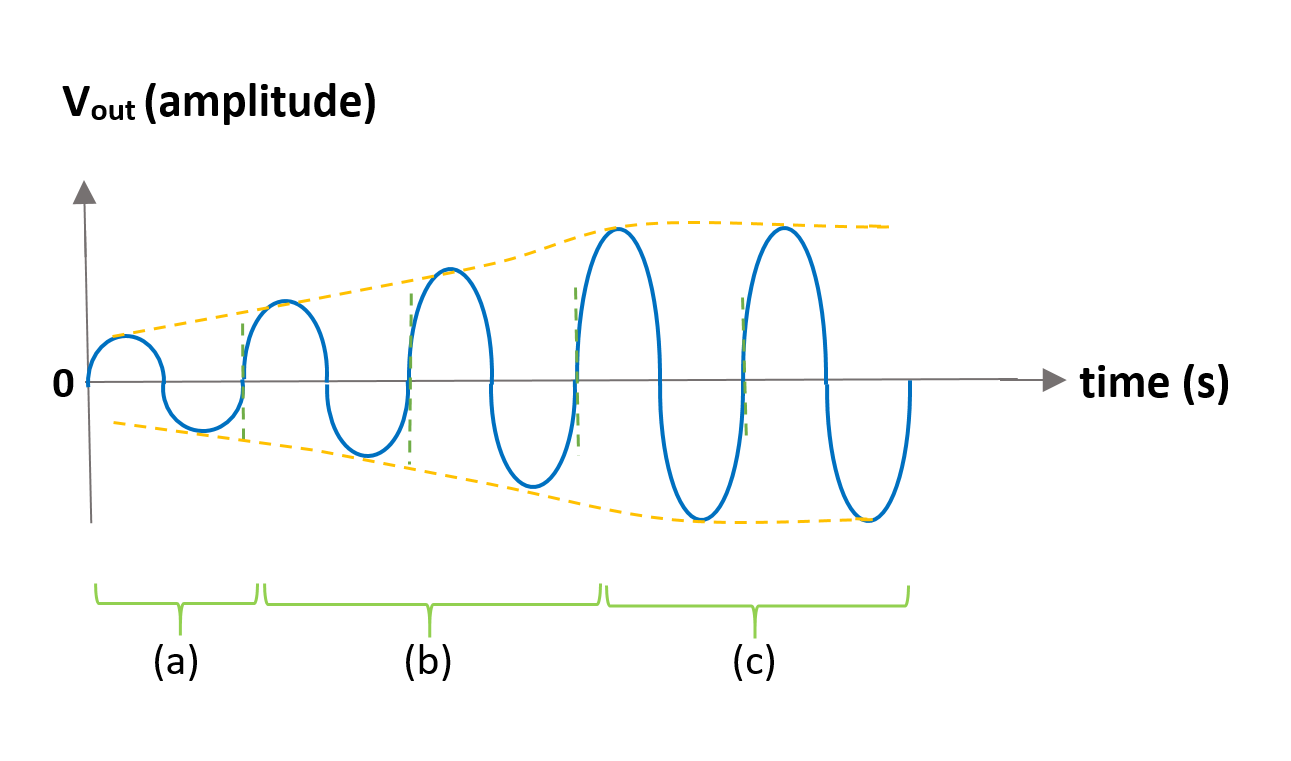
Figure 7: Generation of the periodic waveform due to oscillation in the circuit
Although positive feedback is useful in constructing oscillator circuits, unwanted oscillations render an amplifier useless. Furthermore, electronic circuits often contain unwanted but unavoidable feedback paths. The signals fed back through such paths can deteriorate performance. Similar effects caused by the stray or parasitic capacitance between the parts of an electronic component or circuit are sometimes observed.
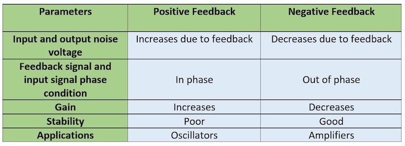
Finally, the features of negative and positive feedback systems are compared in Table 1.
Table 1: Comparison of positive and negative feedback systems
Summary
- In electronics, there is the in-phase relationship between input and output in positive feedback, and the output is fed back to the positive input. This has the effect of increasing the output and going to extremes.
- An op-amp with positive feedback tends to stay in the previous state of its output.
- The hysteresis is an effect very commonly created using a positive feedback loop with an op-amp.
- The use of positive feedback that may result in a feedback amplifier having loop-gain βA equal to or greater than 1 and satisfying the phase conditions will result in its operation as an oscillator circuit. An oscillator circuit then provides a periodic varying output signal.
- Oscillators can be imagined as amplifiers with positive feedback.


