This autofocus camera is tiny, but definitely not to be underestimated: The uEye XS from IDS Imaging Development Systems weighs just 12 grams and fits into almost any application with its size of just 26.4 x 23 x 21.7 mm. Thanks to its autofocus and 5 MP CMOS sensor, it delivers consistently sharp images and videos from a distance of just 10 cm – for example in hand-held scanners, on robotic arms or in passport photo machines. The uEye XS starter set is ideal for testing the camera. In addition to the compact USB2 camera, it includes a cable, a tripod adapter and a tripod.
If the distance between the lens and the object is constantly changing, users benefit from industrial cameras with automatic focus. They eliminate the need for manual refocusing and ensure that objects or labels are always perfectly visible. When it comes to image quality, however, other factors are also decisive, such as natural color reproduction and harmonious contrast.
IDS has therefore equipped the uEye XS with many other practical automatic features familiar from consumer technology. This includes white balance, exposure, and gain. As a result, it delivers the best possible result in every situation. Anyone wishing to fine-tune even more precisely can adjust settings in the SDK (IDS Software Suite).
Thanks to its small size and the proven USB2 interface, the uEyeXS camera is suitable as a component in embedded vision systems. It is used, for example, in medical or security applications, in transport and logistics or in kiosk systems.
iWave introduces iW-RainboW-G63M: a System on Module (SoM) based on the AMD series, targeting next-generation network and cloud deployments. The new SoM features the Versal Premium series rich in networking interfaces, security engines, and high compute density required for a wide range of applications ranging from data centers and 5G to communication test equipment. The System on Modules and evaluation kits from iWave will be available for evaluation starting in December 2024.
iW-RainboW-G63M: The Versal Premium-based System on Module is compatible with an extensive series of chipsets: VP1552/VP1502/VP1402/VP1202/VP1102. The System on Module is integrated with 4GB LPDDR4 RAM, 256MB QSPI Flash, 16GB eMMC Flash, and 4Kbit EEPROM. Three high-speed expansion connectors supporting high speed transceiver channels up to 112Gbps speed and 192 user configurable IOs provided on the System on Module enable a multitude of interfaces available for the user.
The Versal SoM offers networked, power-optimized cores with many high-speed connectivity options like 112Gbps high-speed transceiver blocks providing superior bandwidth, multi-hundred-gigabit ethernet, PCIe Gen5 with built-in DMA, providing the flexibility to support a variety of data rates and protocols.
Versal Premium combines scalar engines (Arm Cortex A72 Cores applications processor and Arm Cortex R5 core for real-time processing and control) enabling compute for complex algorithms while enabling high levels of safety and security. Boasting high-speed cryptography engines, the Versal Premium series delivers 1.6Tb/s of line rate encryption throughput, making it an ideal platform for secure networks. With the System on Module, customers can build network and cloud applications with reduced development cost, reduced risk and time.
Developers can initiate their projects with the Versal Premium evaluation kit. iWave facilitates both hardware and software development with tools like the Vivado design tool, Vitis unified software, frameworks, and accelerated libraries tailored for specific applications. Moreover, iWave offers personalized design and manufacturing services for the SoM, ensuring a holistic ecosystem for customers throughout their product development journey.
“iW-RainboW-G63M System on Module is built to leverage the adaptive portfolio of Versal Premium, enabling the building of fast and secure networks while offering adaptable acceleration for new data-intensive workloads that are transforming networks and data centers,” says Mr. Abdullah Khan M, Director-Engineering at iWave Systems. “The System on Module is an ideal fit for applications like data center interconnect, digital adaptive radars, network testers, metro/core transport, and security appliances where massive serial bandwidth, security, and compute density.”
About iWave
iWave is an embedded systems engineering and solutions company, designing solutions for the Industrial, Medical, Automotive, and Avionics vertical markets. Building on a core competency of embedded expertise since 1999, iWave boasts of an extensive portfolio of high-performance FPGA and SoC FPGA System on Modules and embedded computing platforms enabling customers in their product development journey. Learn more about iWave at www.iwavesystems.com.
After an intensive journey of product research and development, combined with extensive testing, the Croatian-based company Soldered Electronics, specializing in e-ink and low-power technology, is proud to announce the market release of a new generation of e-paper products via a global crowdfunding campaign for the Inkplate 6 MOTION e-paper display.
Inkplate 6 MOTION is open hardware driven by open-source software, already produced in large series, and well-known and accepted among the makers and hardware hackers community due to its multifunctionality and versatility.
Inkplate 6 MOTION is a hackable tool for makers, designers, thinkers, and others ready to take advantage of e-paper display technology. Its adaptability, paper-like aesthetic, daylight readability, and extremely low power consumption make it ideal for a wide range of applications. Whether you’re a creative professional, a product designer, an engineer, a student, a writer, a smart-home enthusiast, or anyone else engaged in creative or technical pursuits, this device supports all kinds of e-paper projects. It’s perfect for displaying photographs, gathering and visualizing data, reading and writing text, or any other application that benefits from the magic of e-paper.
What makes the Inkplate 6 MOTION device truly advanced and innovative is its unmatched speed and ease of use. With its 6.0-inch display capable of refreshing at 11 frames per second, it allows for not only quality images but also smooth video and captivating animations with minimal lag. Paired with a powerful STM32H743 microcontroller and enhanced connectivity options, this Inkplate model excels beyond typical e-paper devices, establishing itself as one of the leading choices among high-end e-paper displays for its superior technical performance.
Video
Inkplate 6 MOTION comes with user-friendly tools that make e-paper accessible without requiring in-depth programming expertise. It supports the Arduino IDE for quick and easy image rendering and leverages MicroPython for more complex projects. Adafruit GFX support is included, as is compatibility with the Home Assistant and ESPHome automation platforms.
With its multifunctionality and numerous features, Soldered Electronics invites you to explore the Inkplate 6 MOTION in more detail on its crowdfunding campaign page and video presentation.
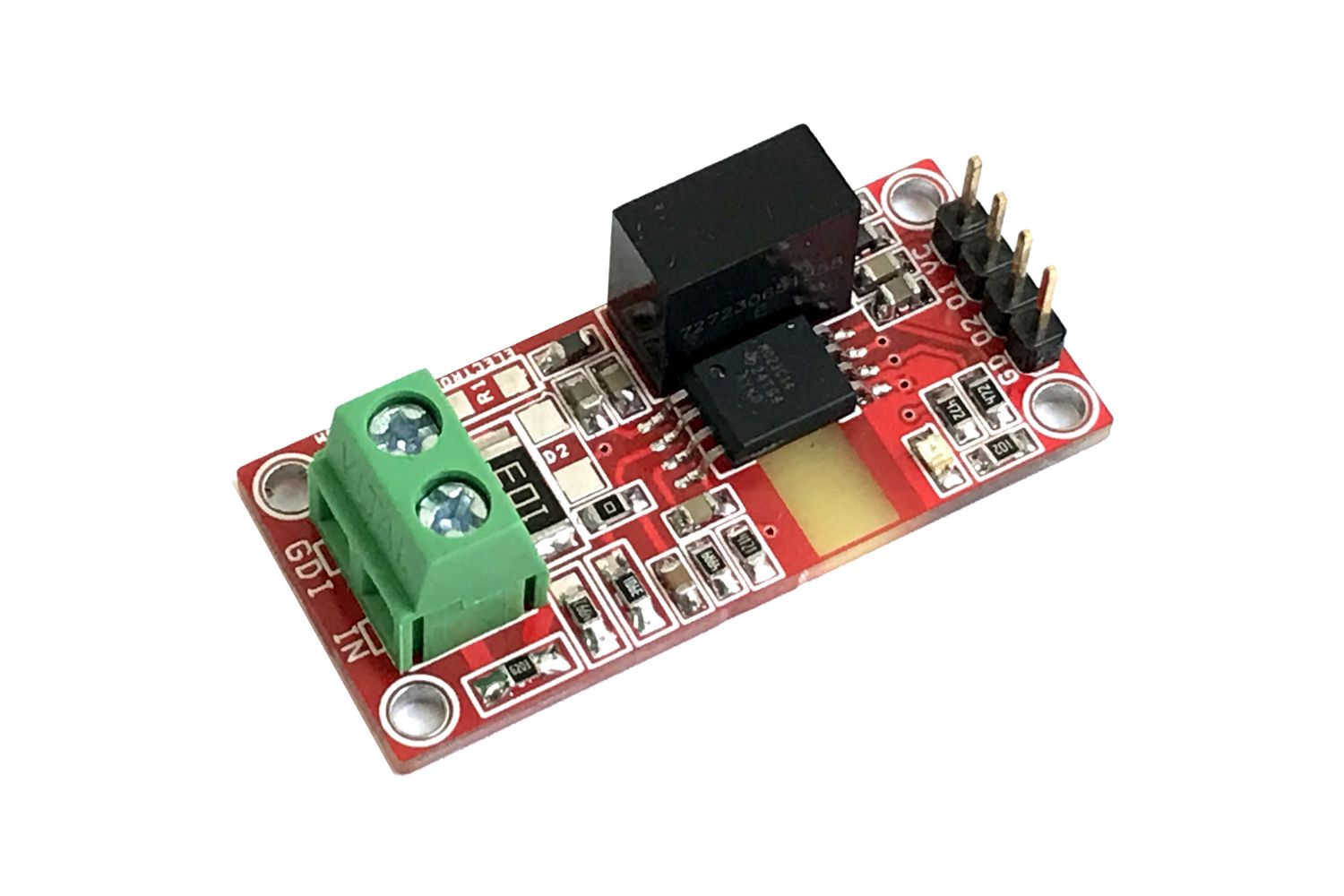
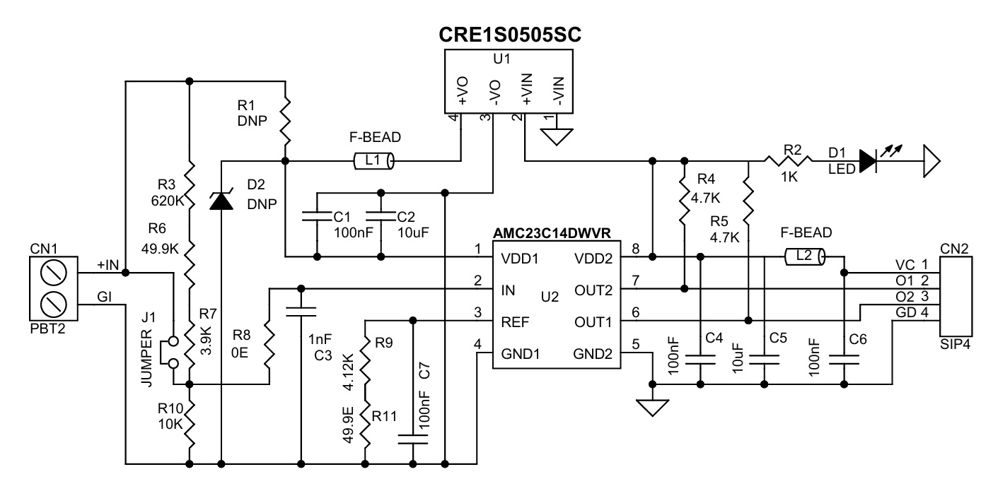
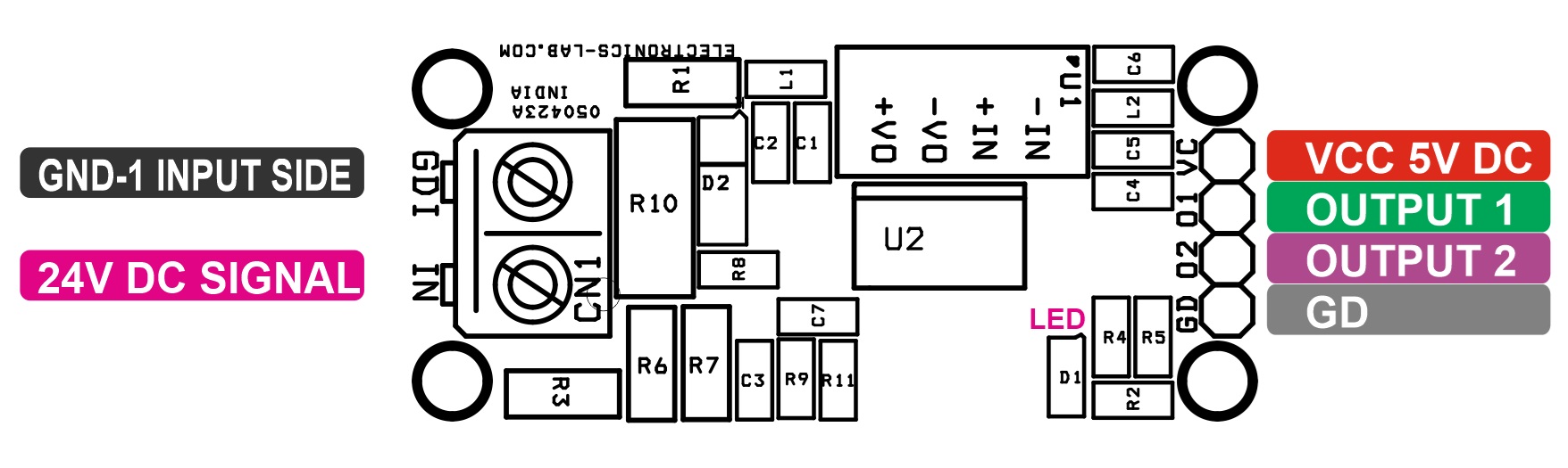
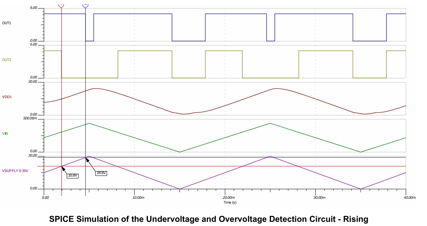
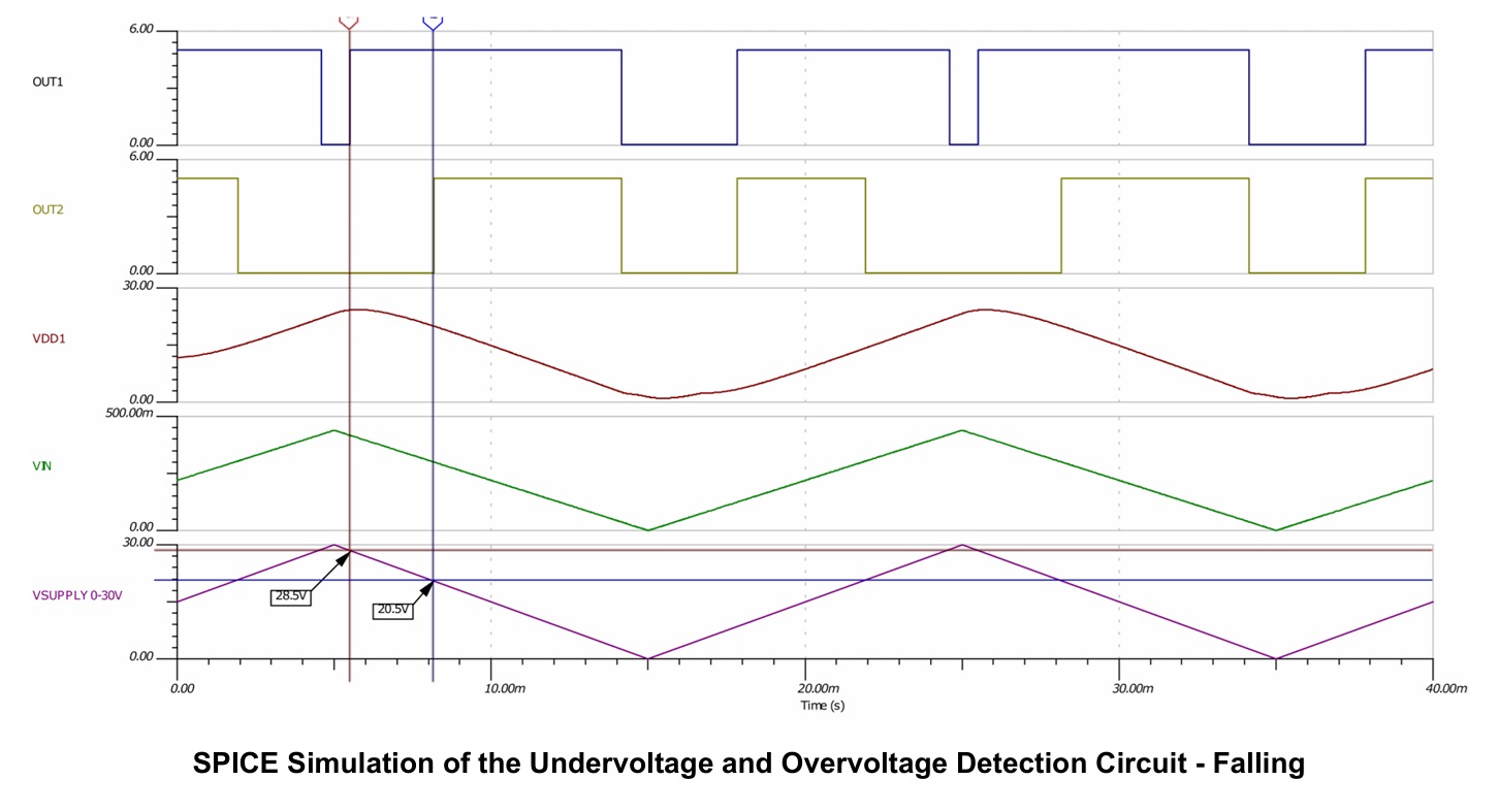
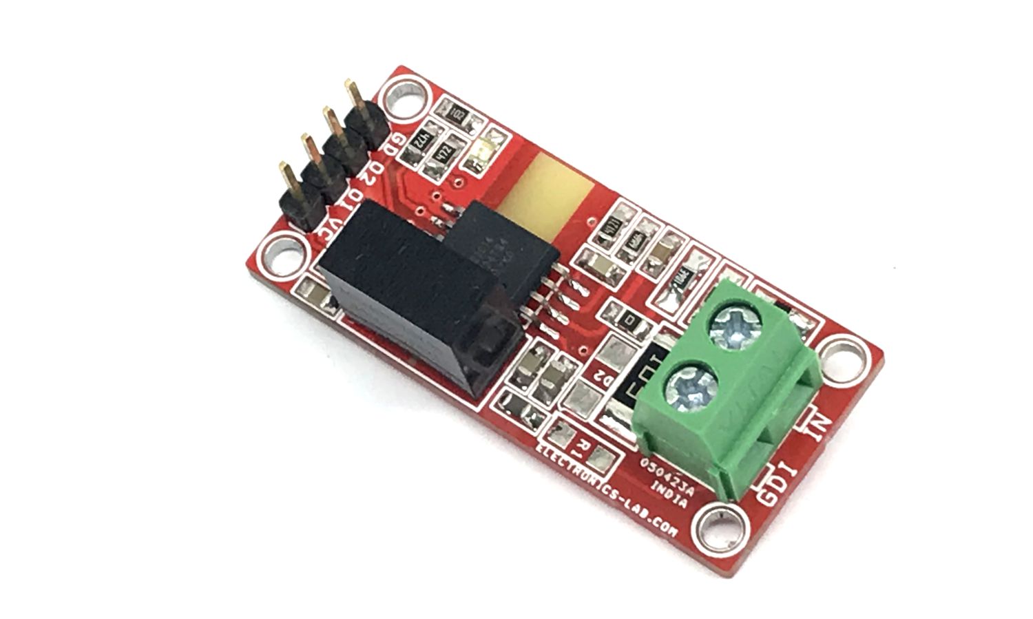
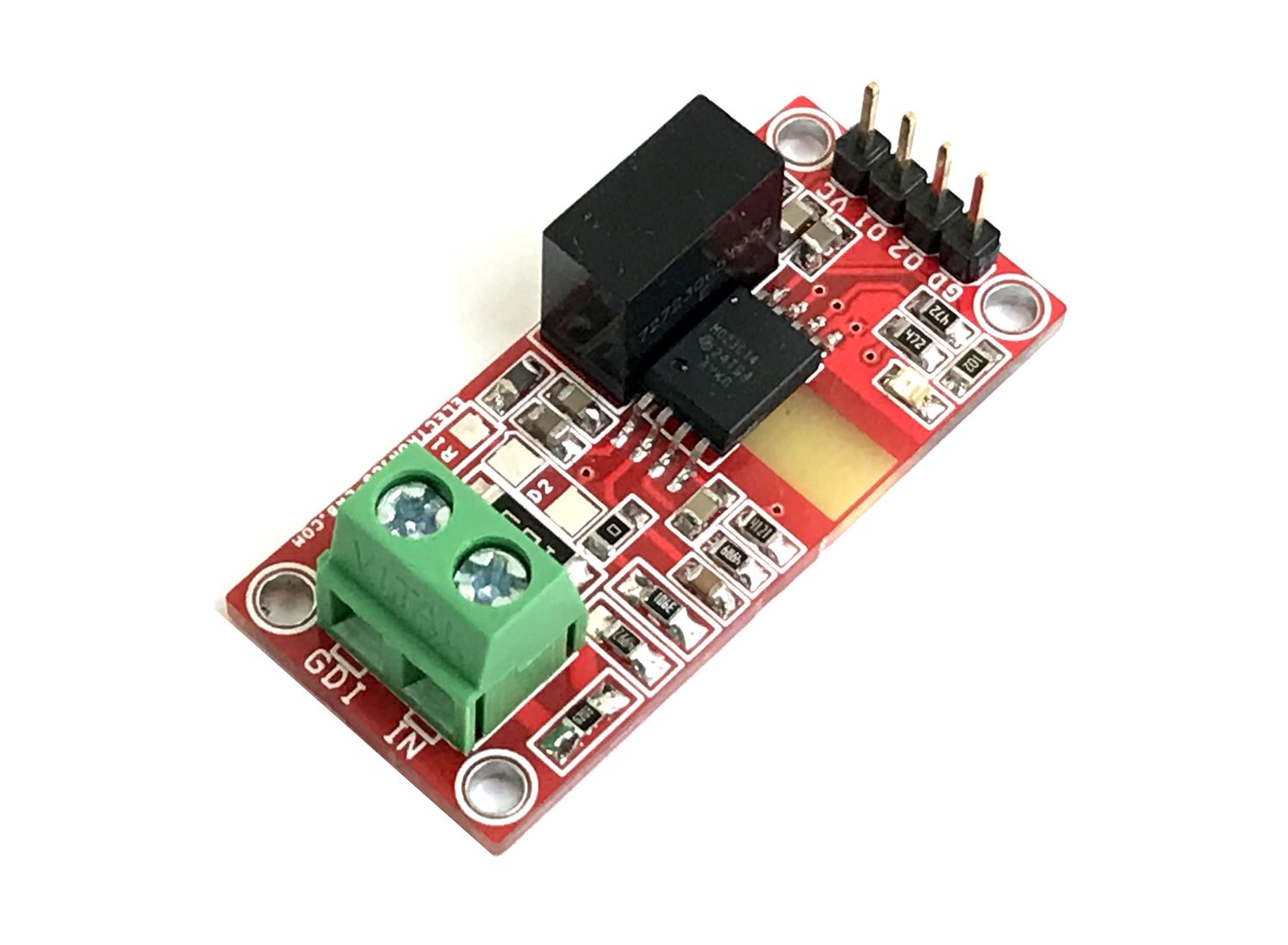
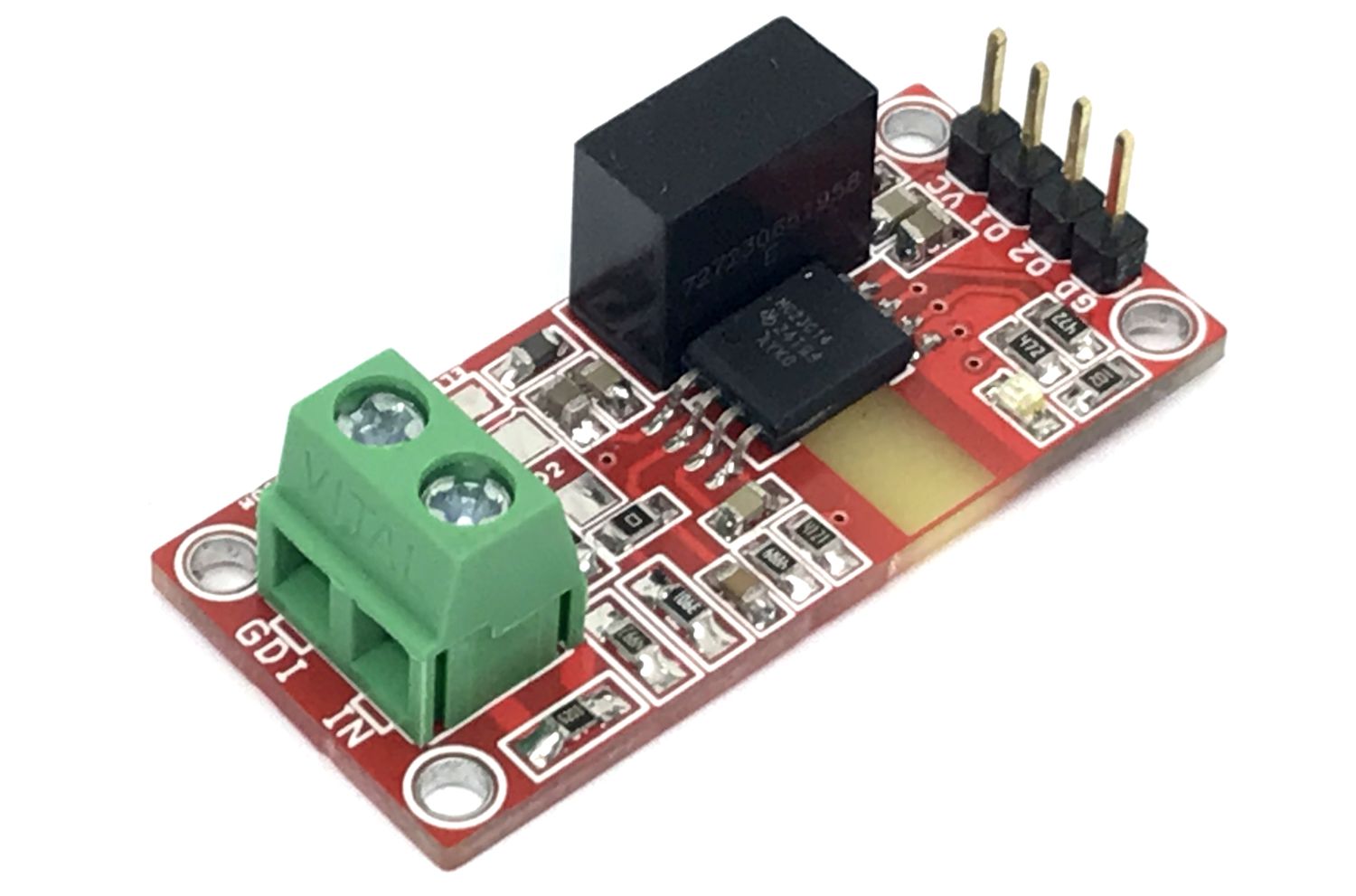
This high-speed, isolated Undervoltage and Overvoltage detection project is implemented with a dual isolated window comparator with an adjustable threshold (AMC23C14). This circuit is designed for industrial field-supply applications where the controller side must detect whether the remote module supply voltage is in a valid range.
The AMC23C14 has open-drain outputs that are pulled up to VCC, and are driven low when the input voltage exceeds the threshold voltage of each comparator. In these measurements, OUT1 (trace 3) transitions low if Vsupply exceeds 28.8V, and OUT2 transitions low if Vsupply exceeds 20.8V. Component variations and the comparator hysteresis can affect the trip thresholds, but in this case, the trip point is within less than 1% of the desired values. The voltage thresholds vary slightly if Vsupply is rising or falling. The second waveform depicts this with OUT1 triggering at 28.6V instead of 28.8V.
U1 (CRE1S0505SC) is an isolated DC-DC converter that provides 5V to the input side circuitry. The module can be powered from input side power, using R1 1K SMD size 0805 and Zener diode 27V 1W SMD. Do not install U1 in this case, the output side requires separate 2.7V to 5.5V VCC.
Over Current and Short Circuit Application
The project is designed for Under/Over voltage detection. However, the project also has provisions to be used for over-current and short-circuit detection. Read the datasheet of the chip for more info. Do not install R3, R6, and R7, Install R10 = 10mOhms SMD size 2512, solder jumper J1 under the PCB. This configuration will help you to detect over current and short circuit across the shunt resistor R10.
Features
Power Supply 5V DC
Input Signal 24V
Over Voltage Level 28.8V
Under Voltage Level 20.4V
Output 1 and Output 2 Normally High, Low when Over/Under Condition Occurs
7000-VPK reinforced isolation per DIN EN IEC 60747-17 (VDE 0884-17)
5000-VRMS isolation for 1 minute per UL1577
5 mm Mounting Hole
PCB Dimensions 42.23 x 19.05mm
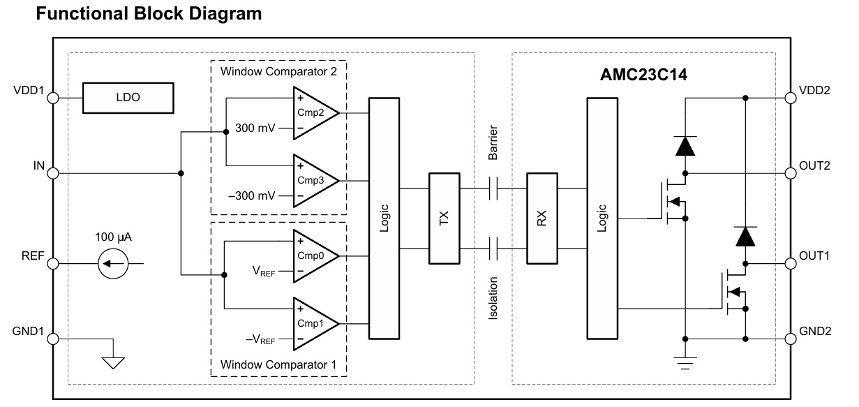
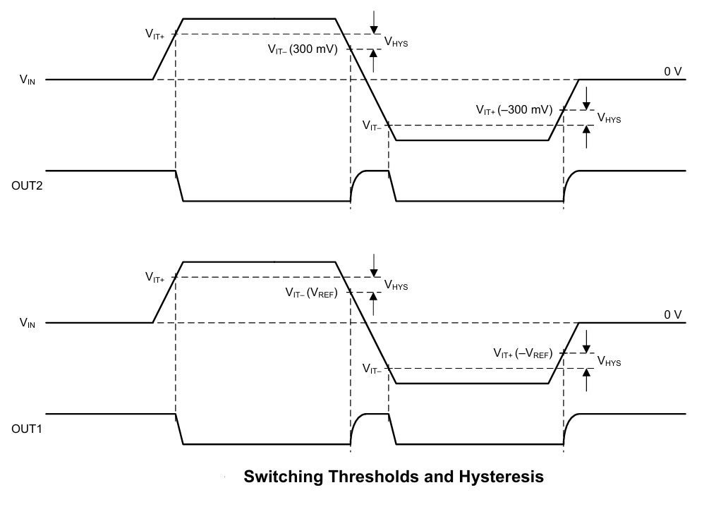
The AMC23C14 is a dual, isolated window comparator with a short response time. The open-drain outputs are separated from the input circuitry by an isolation barrier that is highly resistant to magnetic interference. This barrier is certified to provide reinforced galvanic isolation of up to 5 kVRMS according to VDE 0884-17 and UL1577, and supports a working voltage of up to 1 kVPK.
Both comparators have windows that are centred around 0 V, meaning that the comparators trip if the input exceeds the thresholds in a positive or negative direction. One comparator has fixed thresholds of ±300 mV. The second comparator has adjustable thresholds from ±20 mV to ±300 mV through a single external resistor.
The AMC23C14 also supports a positive-comparator only mode. When the voltage on the REF pin is greater than 550 mV, the negative comparators are disabled and only the positive comparators are functional. The reference voltage in this mode can be as high as 2.7 V. This mode is particularly useful for monitoring positive voltage supplies.
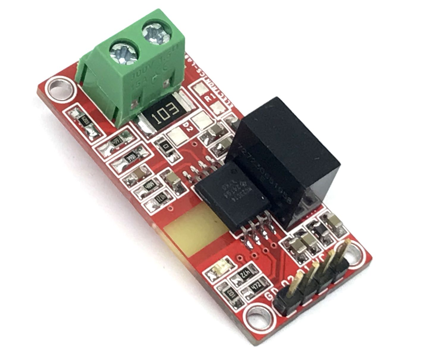
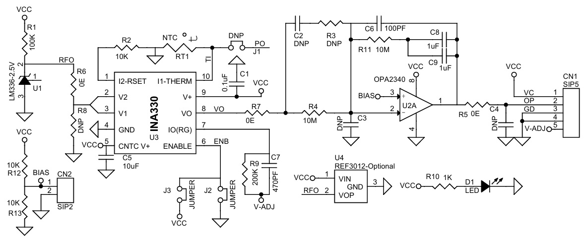
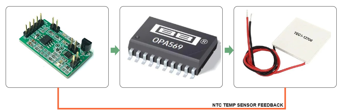
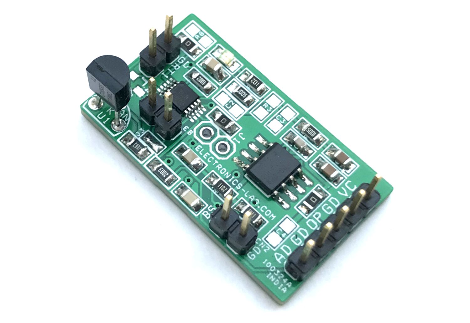
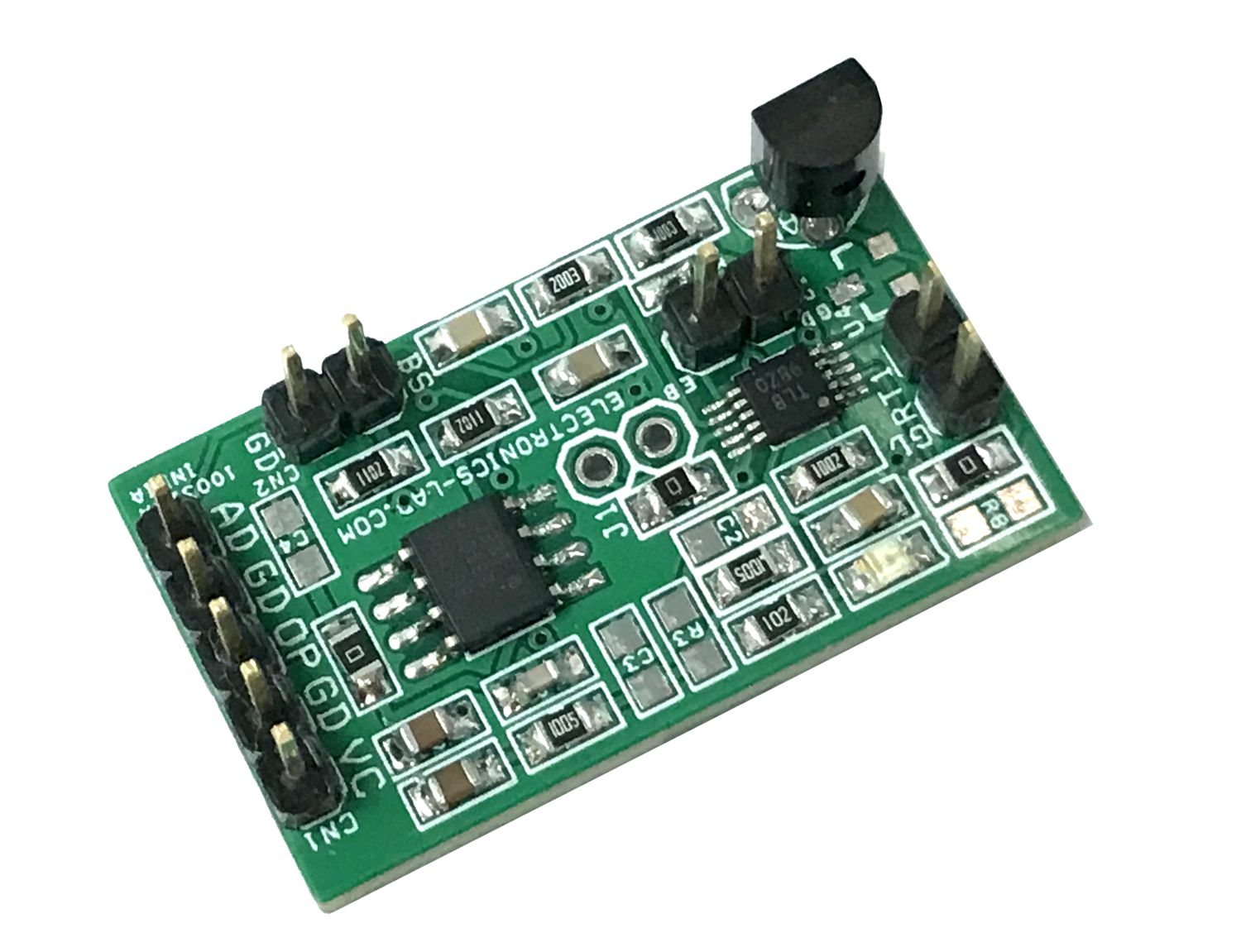
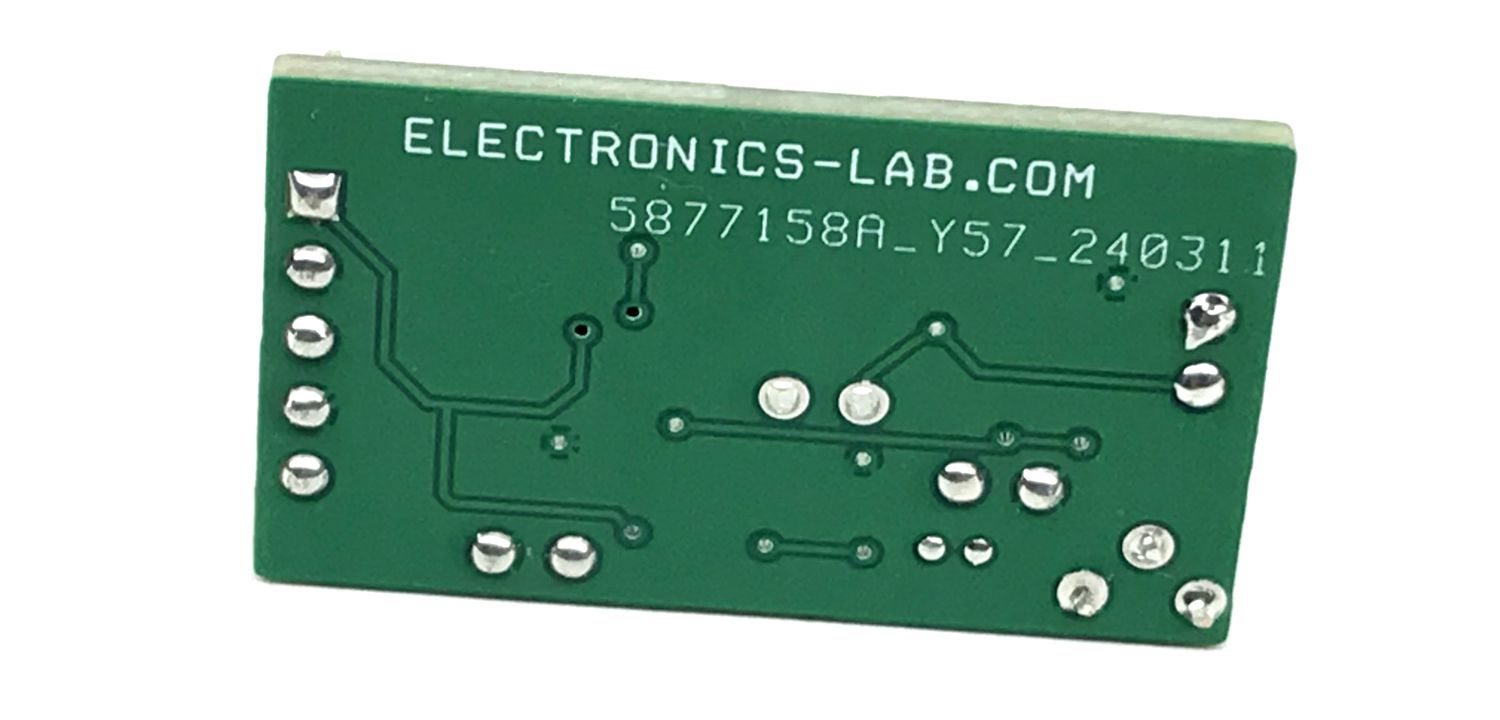
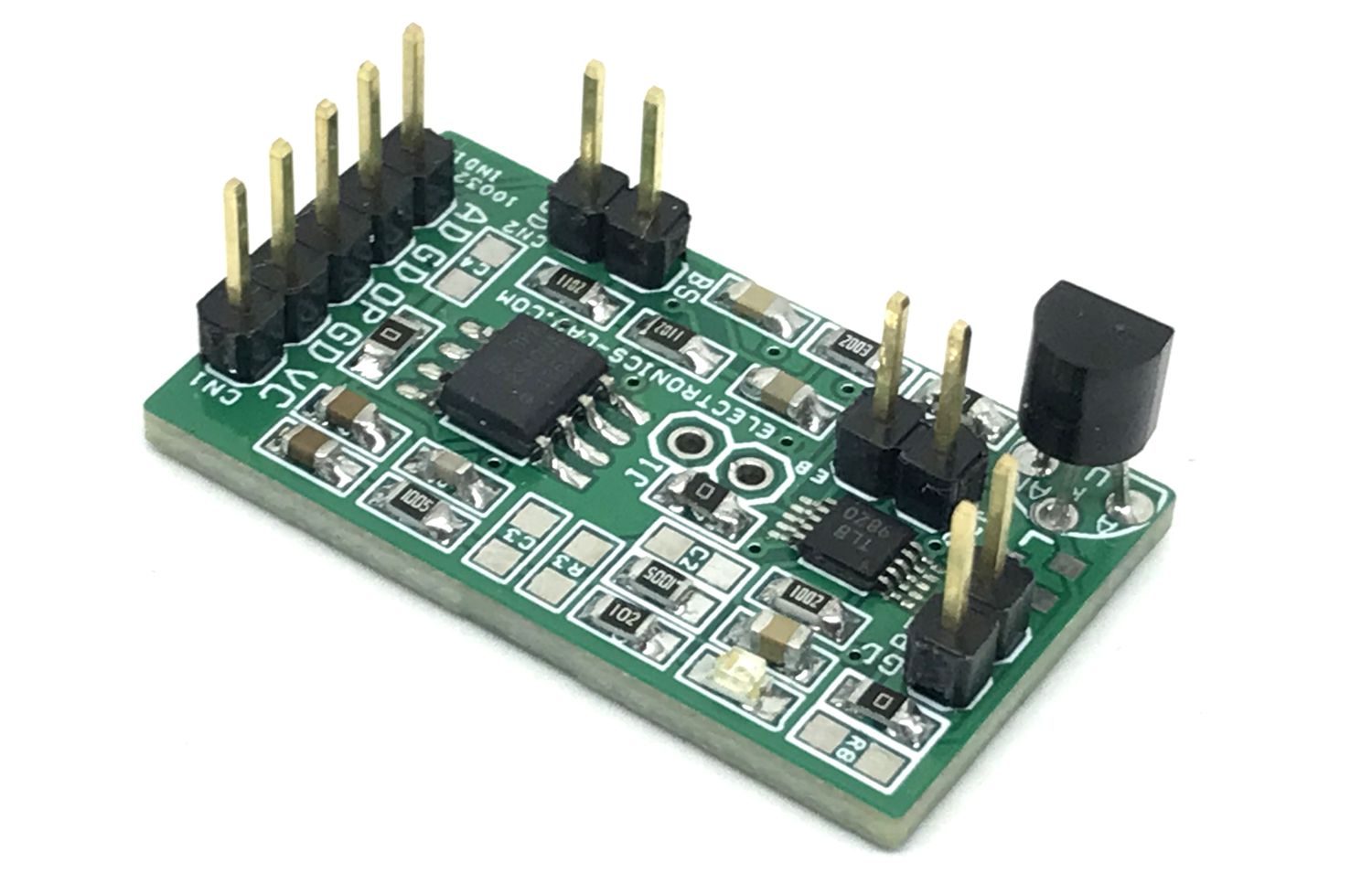
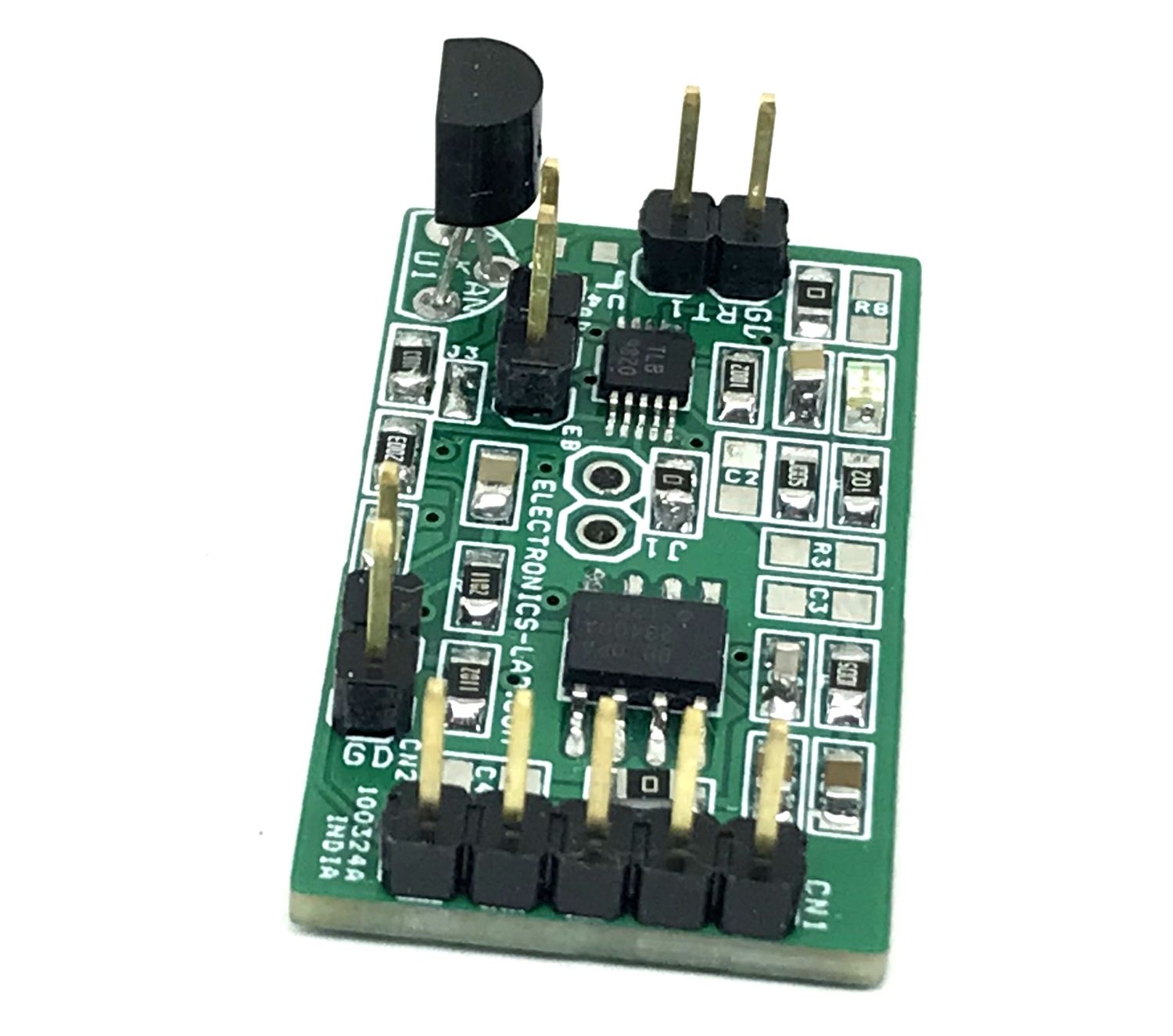
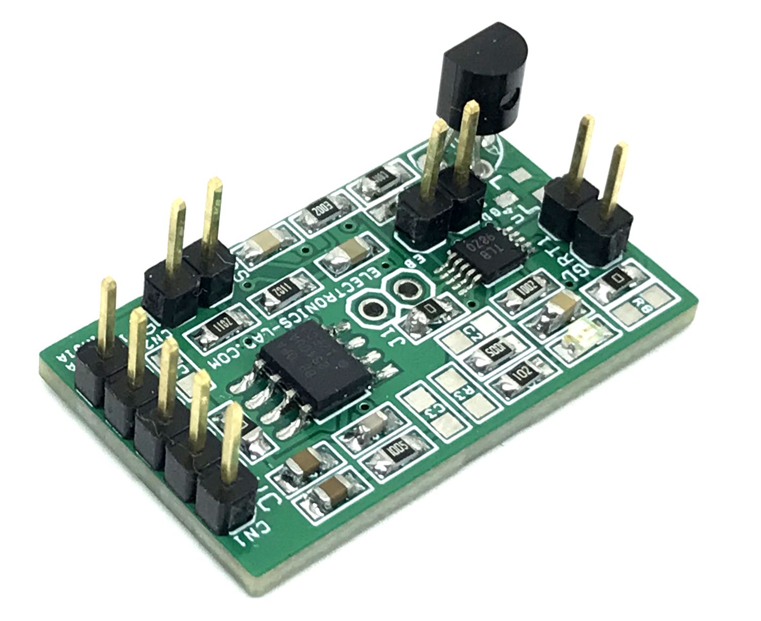
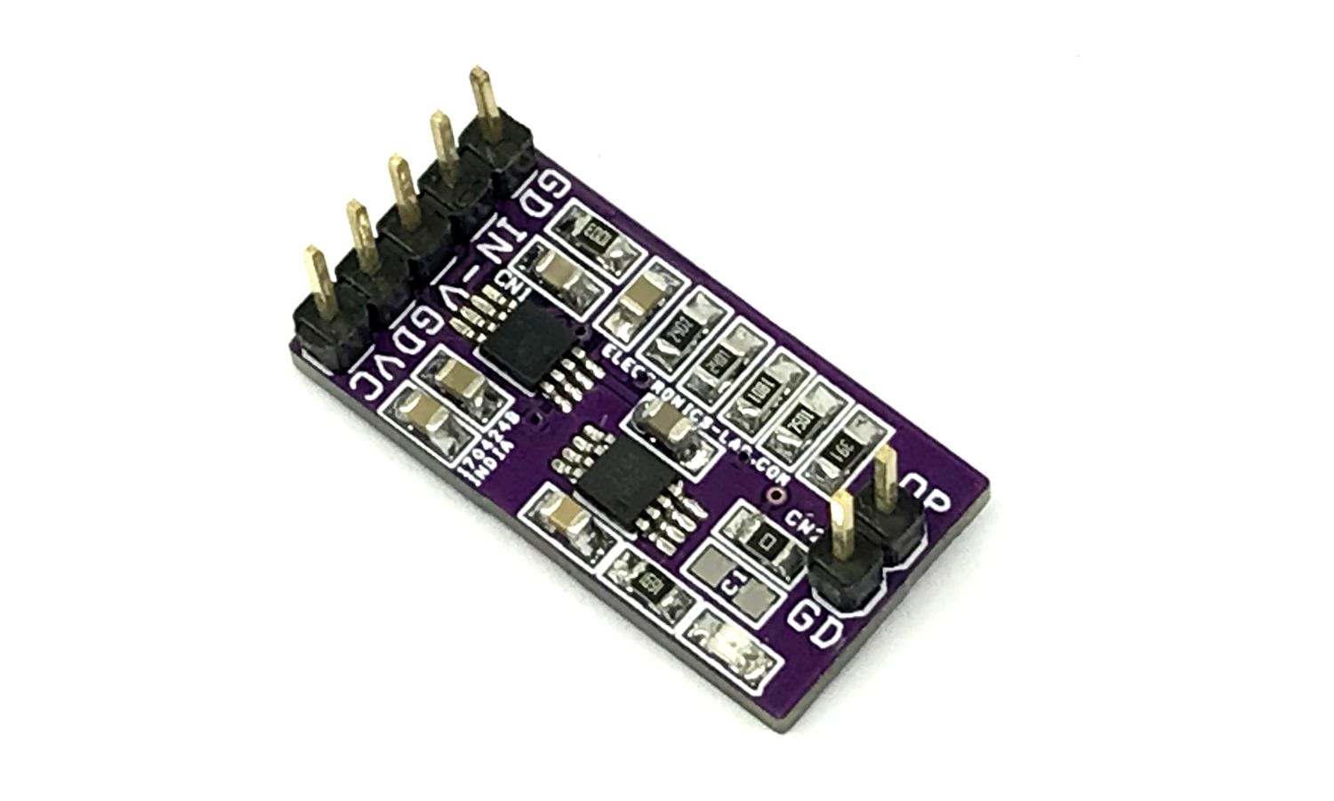
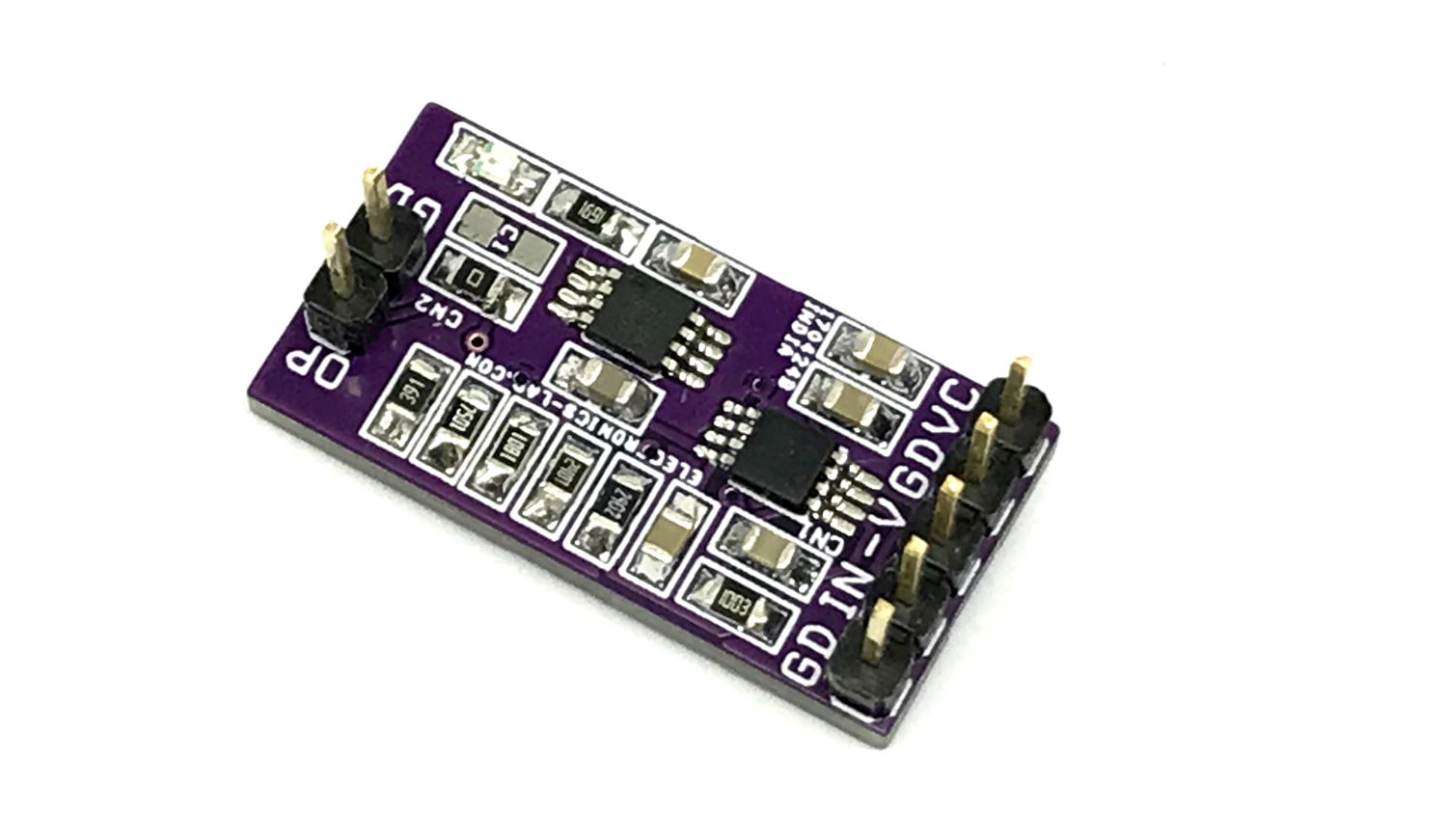
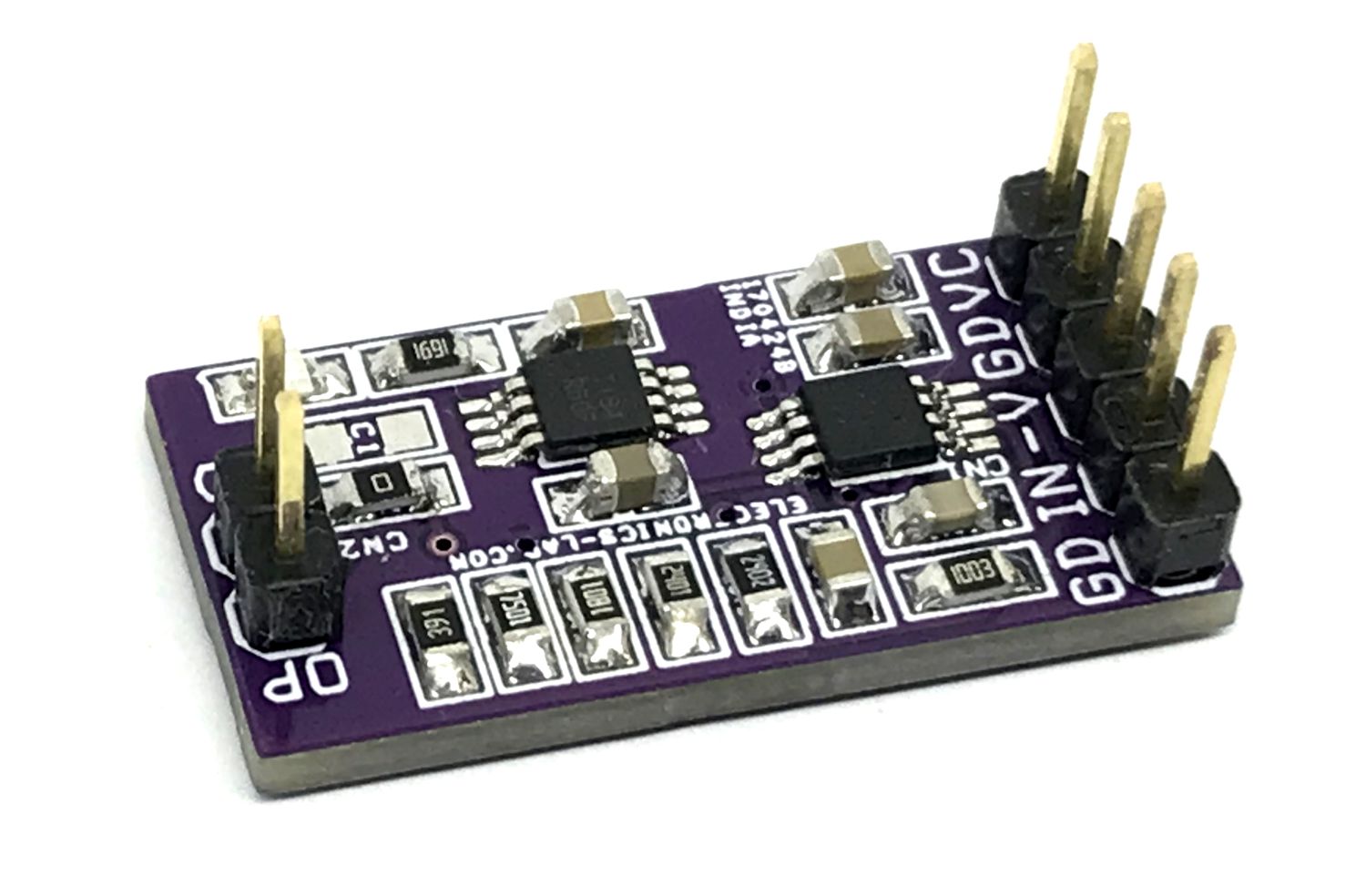
This is a simple Proportional, Integral (PI) temperature control amplifier. A complete thermoelectric cooler (TEC) controller can be created using this PI amplifier and OPA569 Power Op-Amp or other output amplifiers such as DRV591, DRV592 and DRV593. Proportional-integrator compensation is simpler to adjust and often provides an adequate thermal transient response to the TEC driver amplifiers. The project consists INA330 chip and OPA2340 OPAMP. The INA330 provides thermistor excitation and generates an output voltage proportional to the difference in resistances applied to the inputs. OPA2340 is used to create the PI closed Loop.
The board is based on application note Figure 8 from the datasheet of INA330. Please Refer to the datasheet of INA330 to learn more about the project and applications.
U1 LM385-1.2V generates the reference voltage 1.23V, and REF3012 SOT23-2 U4 chip can be used as an alternative to U1. PI loop compensation can be optimized for loop stability and best response to thermal transients by adjusting R4, R11, C8, and C9. To facilitate the optimization of loop dynamics, the value of these components is important and will depend on the Thermal behavior of the TEC.
Features
Supply 5V DC
NTC Temperature Sensor
Compact Design
Precision Temperature Sensor Amplifier
On Board 1.23V Reference
On Board Power LED
PCB Dimensions 31.75 x 18.42 mm
INA330 uses only one precision resistor R2 plus the thermistor RT1, thus providing an alternative to the traditional bridge circuit. The circuit maintains excellent accuracy for temperature control applications. An excitation voltage is applied to the thermistor (RTHERM) RT1 and precision resistor (RSET) R2, creating currents I1 and I2. The current conveyor circuit produces an output current, I0, equal to I1 – I2, which flows through the external gain-setting resistor. A buffered voltage output proportional to I0 is also provided. The loop controls temperature to an adjustable set-point of 22.5°C to 27.5°C. The nominal 10kΩ at 25°C thermistor ranges from approximately 11.4kΩ to 8.7kΩ over this range. A 1.23V excitation voltage is applied to V1 and V2, producing a nominal 100µA current in the 10kΩ RSET resistor. The thermistor current is approximately 100µA at 25°C, but will vary above or below this value over the ±2.5°C set-point temperature range. The difference of these two currents flows in the gain-set resistor, RG. This produces a voltage output of approximately 0.9V/°C. The set-point temperature is adjusted with VADJ. Thus, the voltage at VO is the sum of (IO)(RG) + VADJ. VADJ can be manually adjusted or set with a Digital-to-Analog (D/A) converter. Optionally, Thus, the feedback loop will drive the heating or cooling of the TEC to force VO to equal VBIAS. VADJ = 2.5V will produce a set-point temperature of 25°C. VADJ = 2.5V + 0.9V will change the set-point by 1°C. A 0V to 5V D/A converter will provide approximately ±2.5°C adjustment range. A 12-bit D/A converter will allow for approximately 0.001°C resolution on the set-point temperature. For best temperature stability, the set-point temperature voltage should be derived ratiometrically from VBIAS. A D/A converter used to derive the set-point voltage should share the same reference voltage source as VBIAS. Likewise.
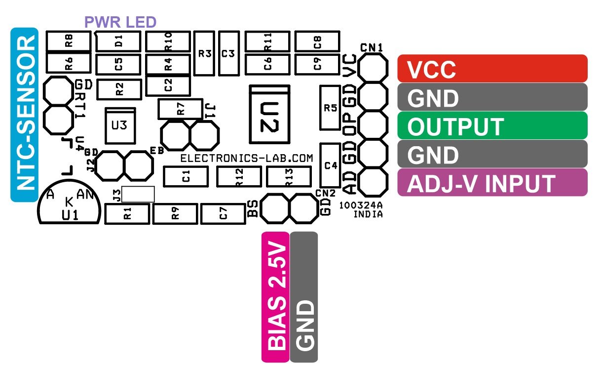
Connections and Other Information
CN1: Pin 1 = 5V DC, Pin 2 = Output, Pin 3 = GND, Pin 4 = GND, Pin 5 = V-ADJ 0 to 5V from DA Converter
CN2: For High Accuracy Omit R12 and R13 and Feed 2.5V External Reference Voltage to Pin 1 , Pin = GND
J1: No Use
J2: Disable
J3: Enable (Solder Jumper)
U1: Reference Voltage Generator, Use Alternate U4 REF3012 SOT23-3
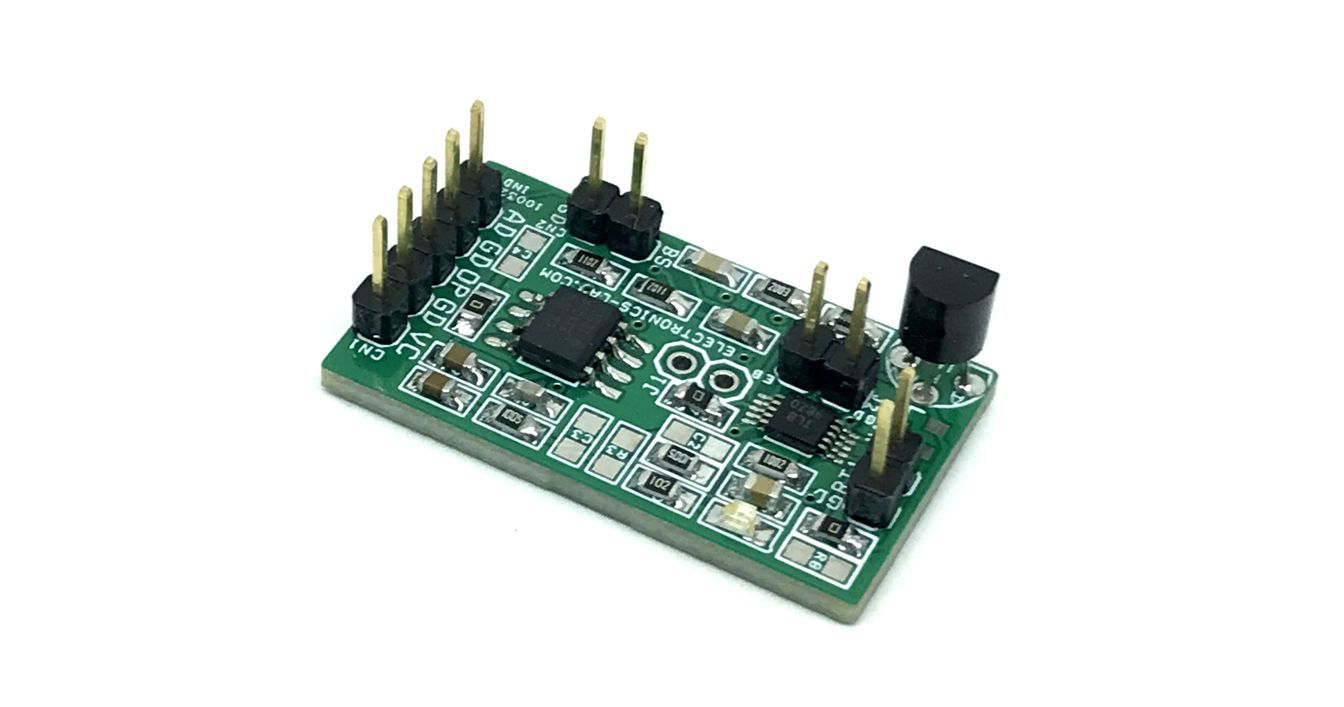
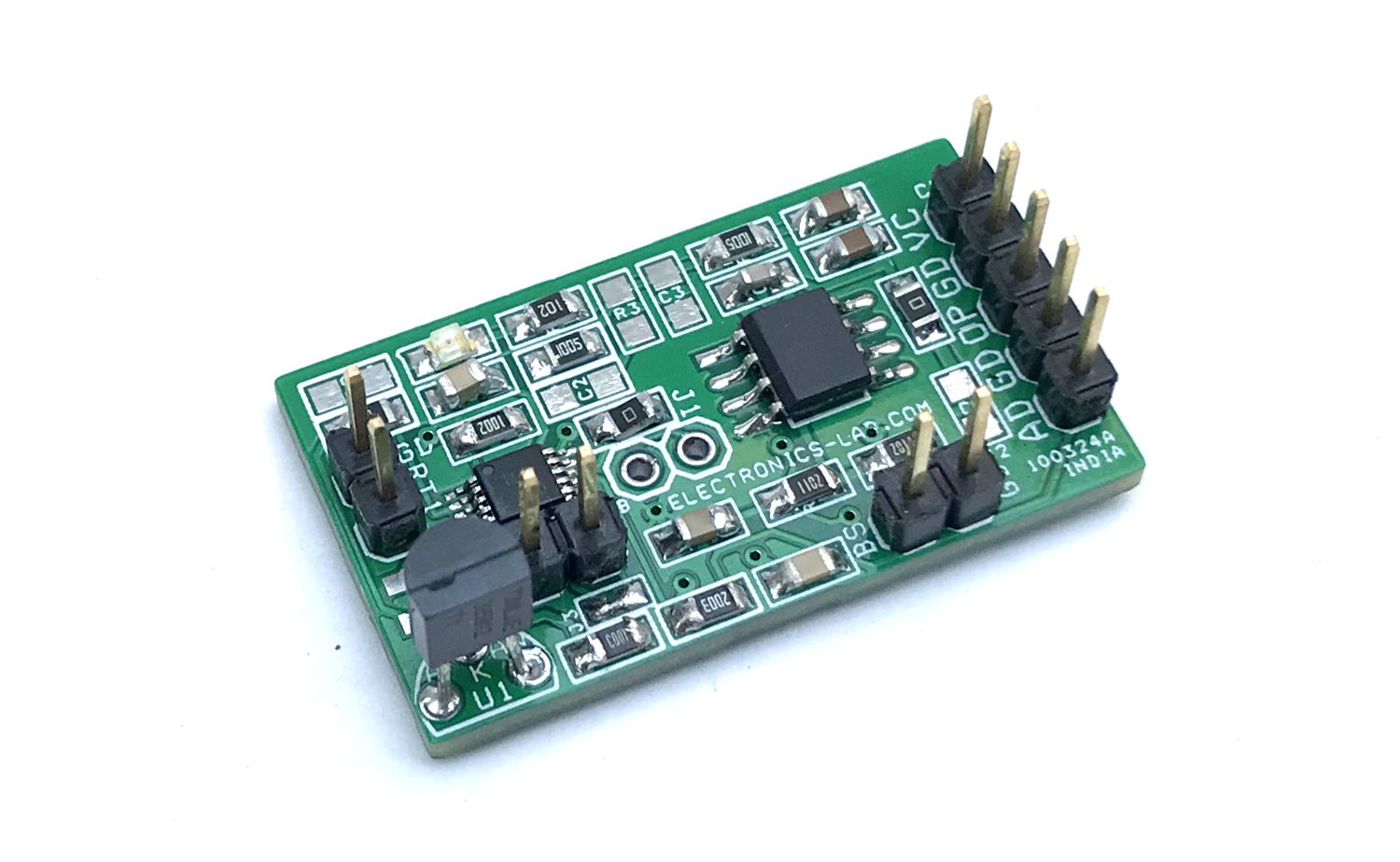
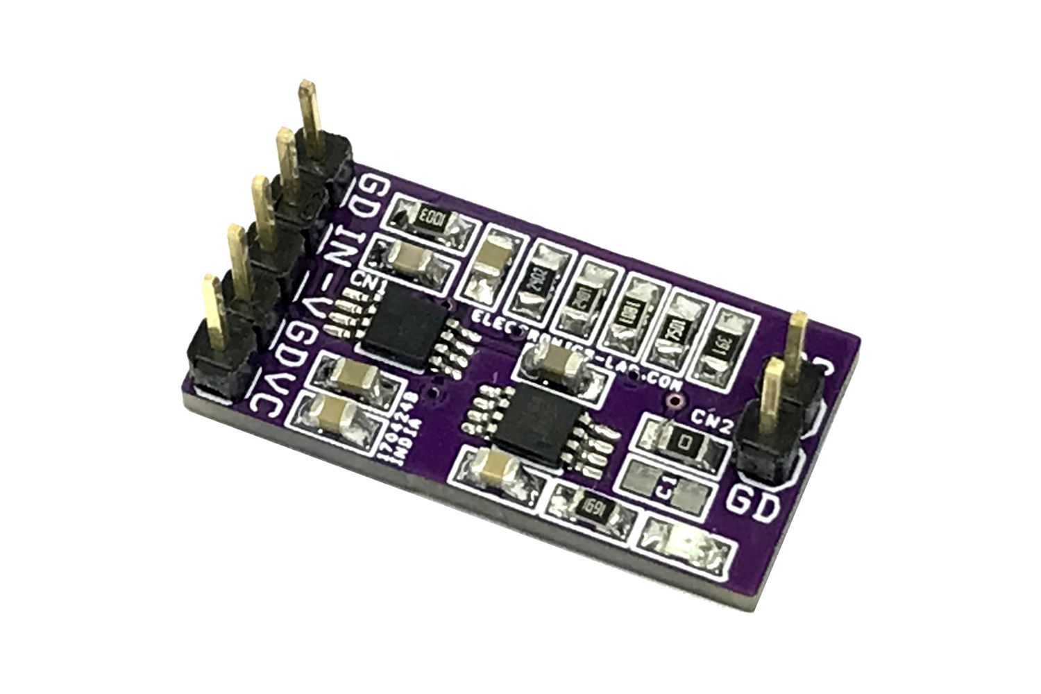
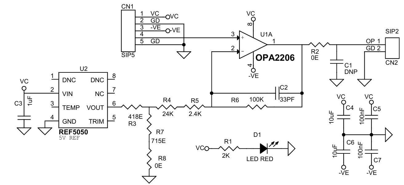
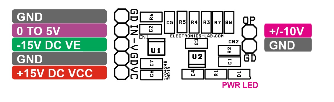
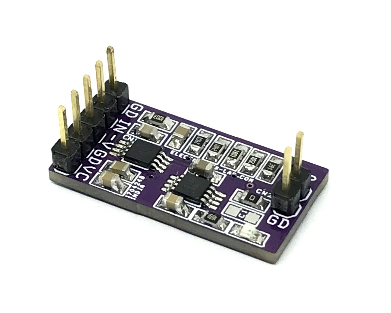
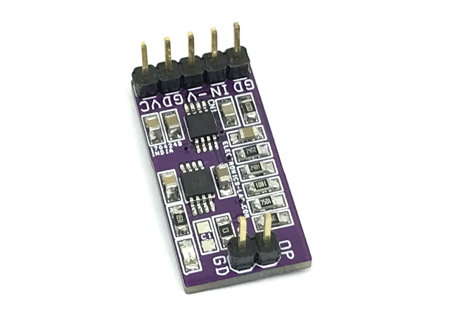
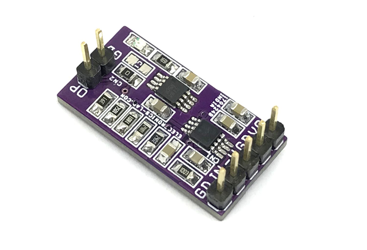
This design is intended to translate a small unipolar signal to a wide bipolar signal. A common application is to translate a 0 to 5V DAC output to a ±10V bipolar signal. All resistors are 1% but it is advisable to select 0.1% 20 ppm/°C resistors for good gain, offset accuracy, and drift tolerance. A calibration at room temperature can be done to minimize the gain error, but gain drift can only be reduced by minimizing the resistor drift (choosing resistors with TC ≤ 20 ppm/°C). The project is built using OPA2206 Precision, bipolar, e‑trim OPAMP. REF5050 provides 5V reference voltage to OPAMP. The board works with a dual ±15V DC Power Supply.
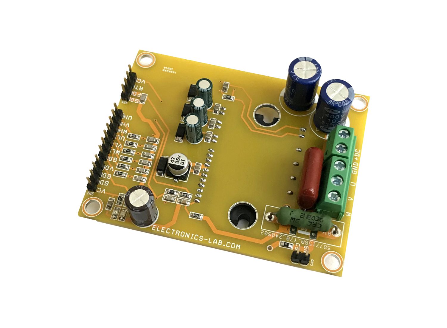
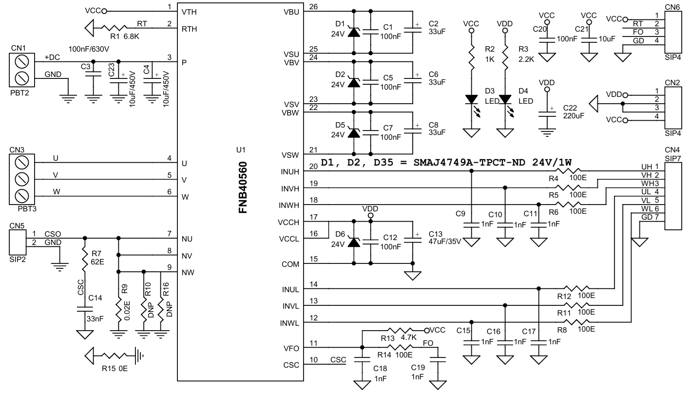
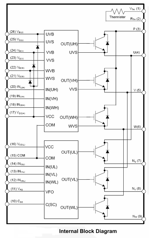
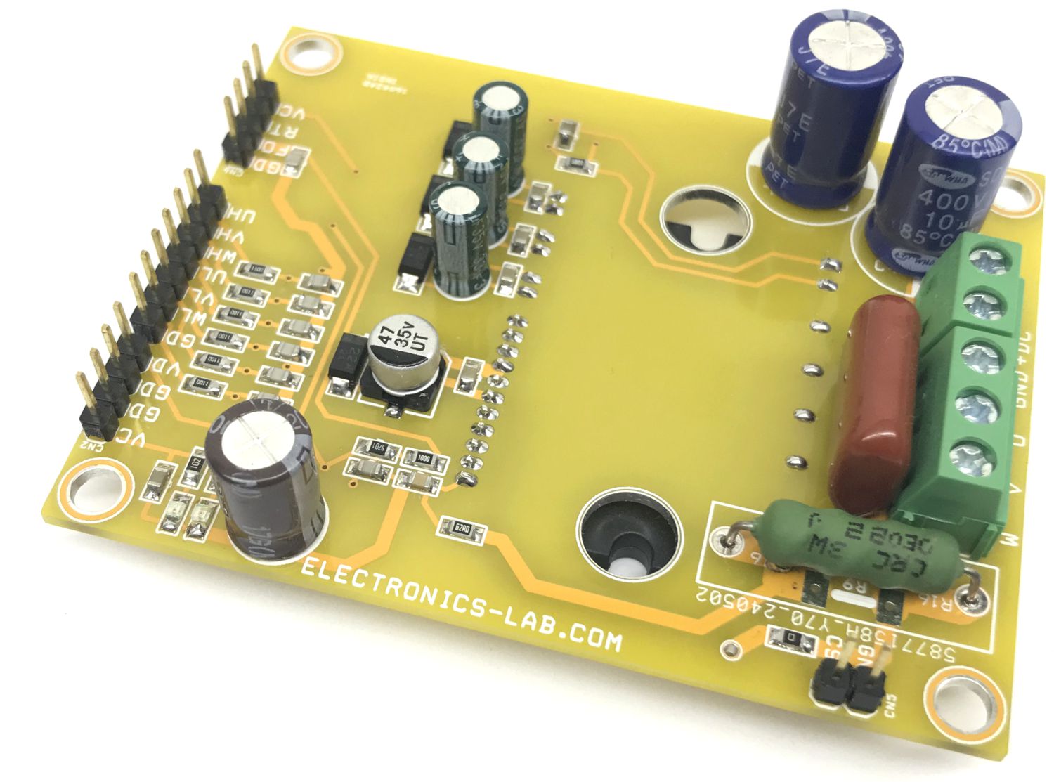
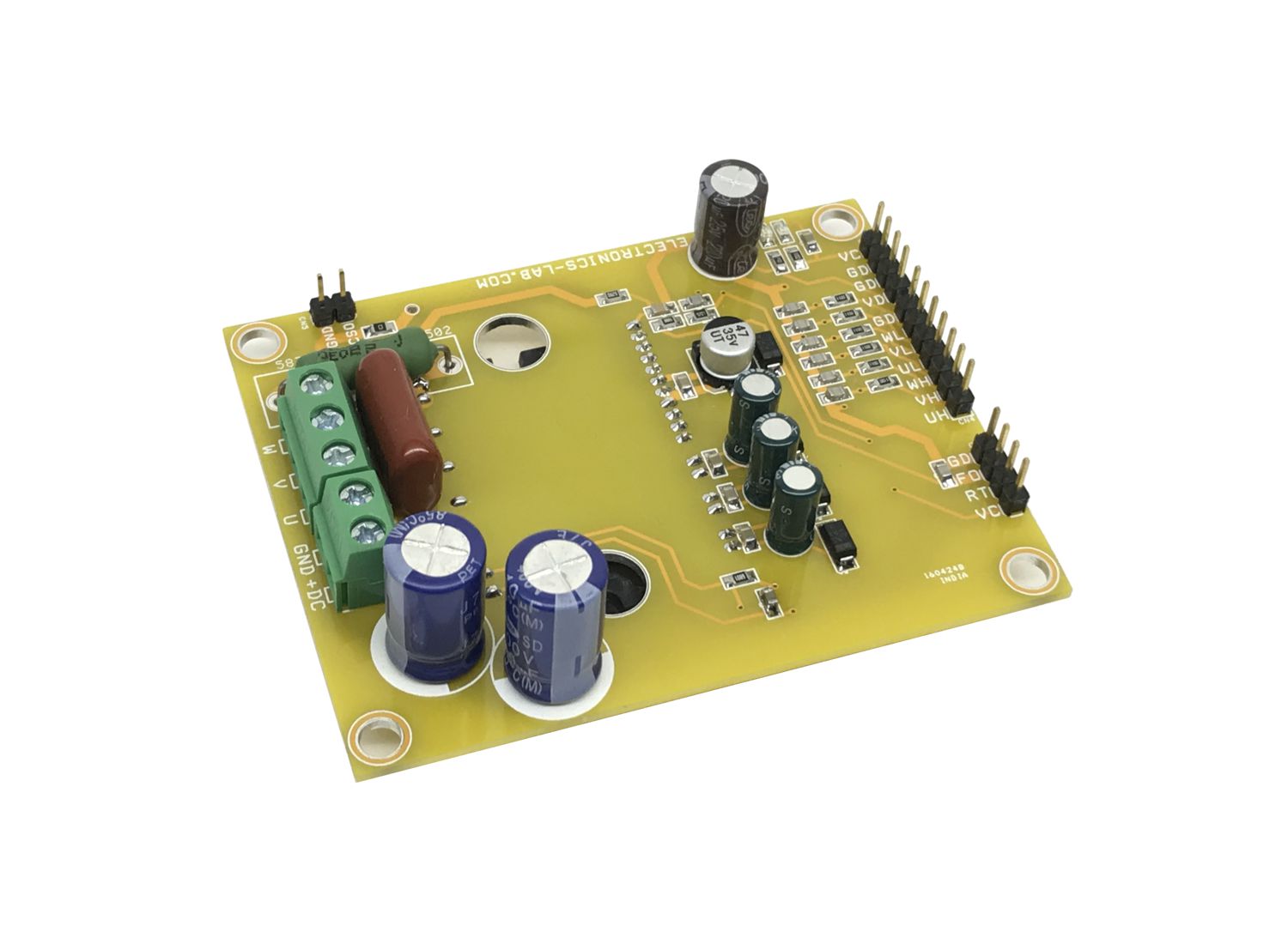
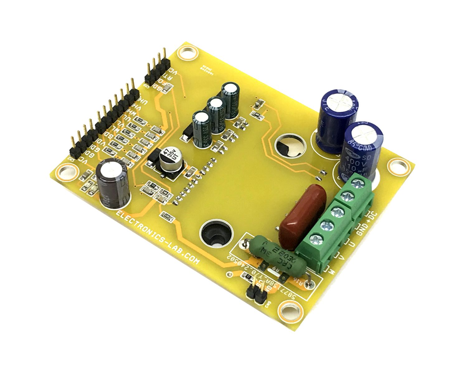
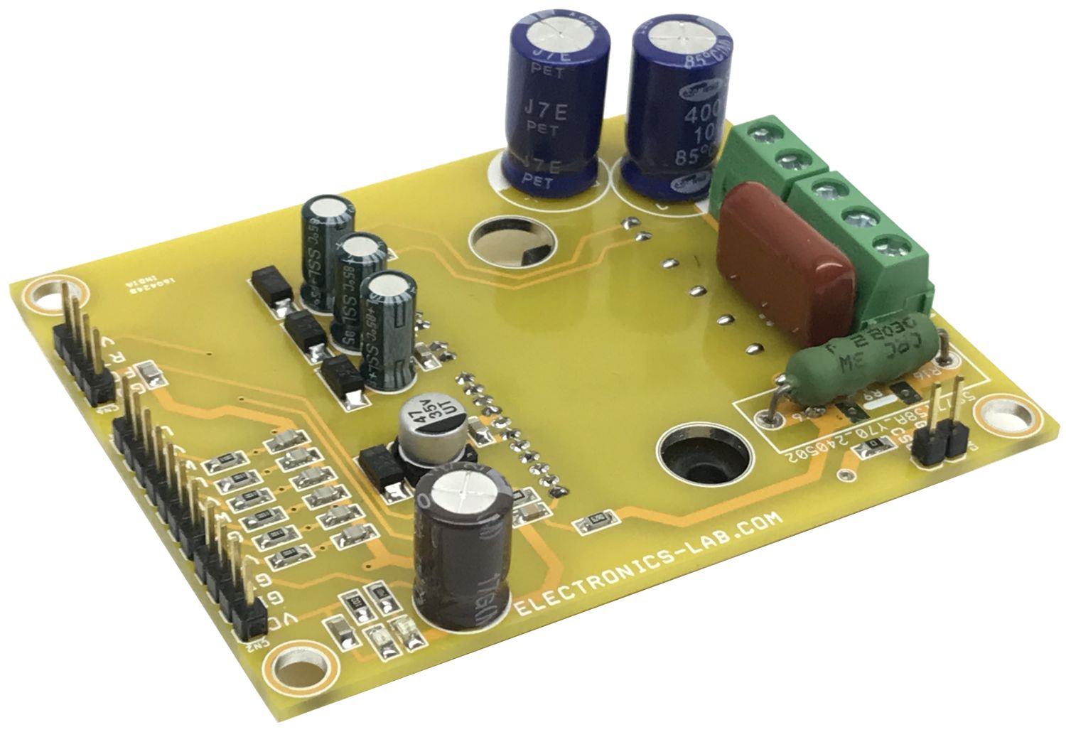
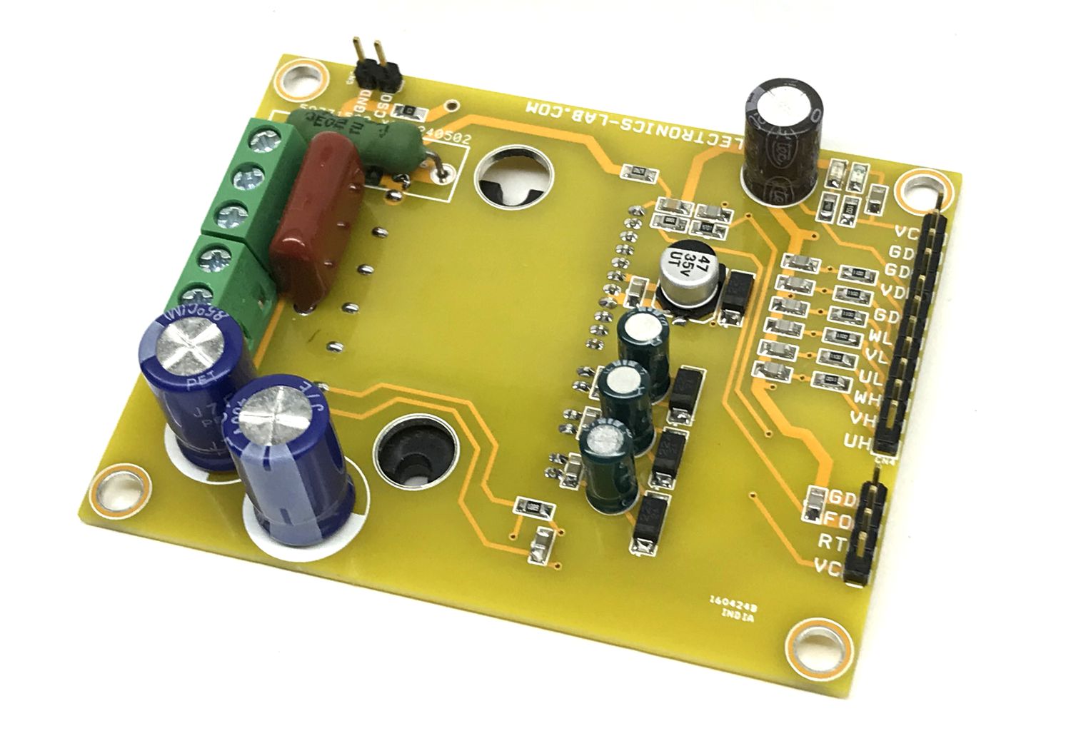
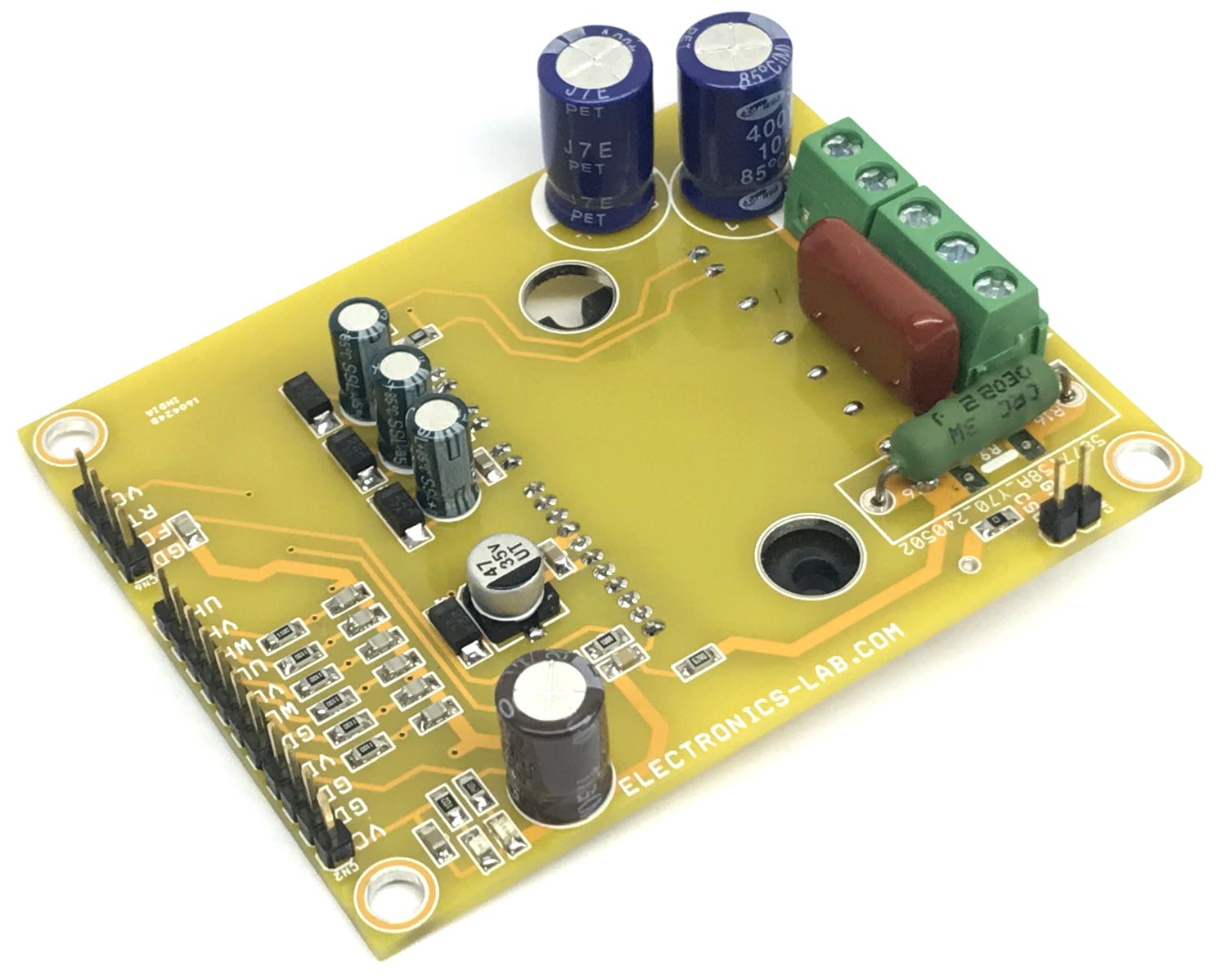
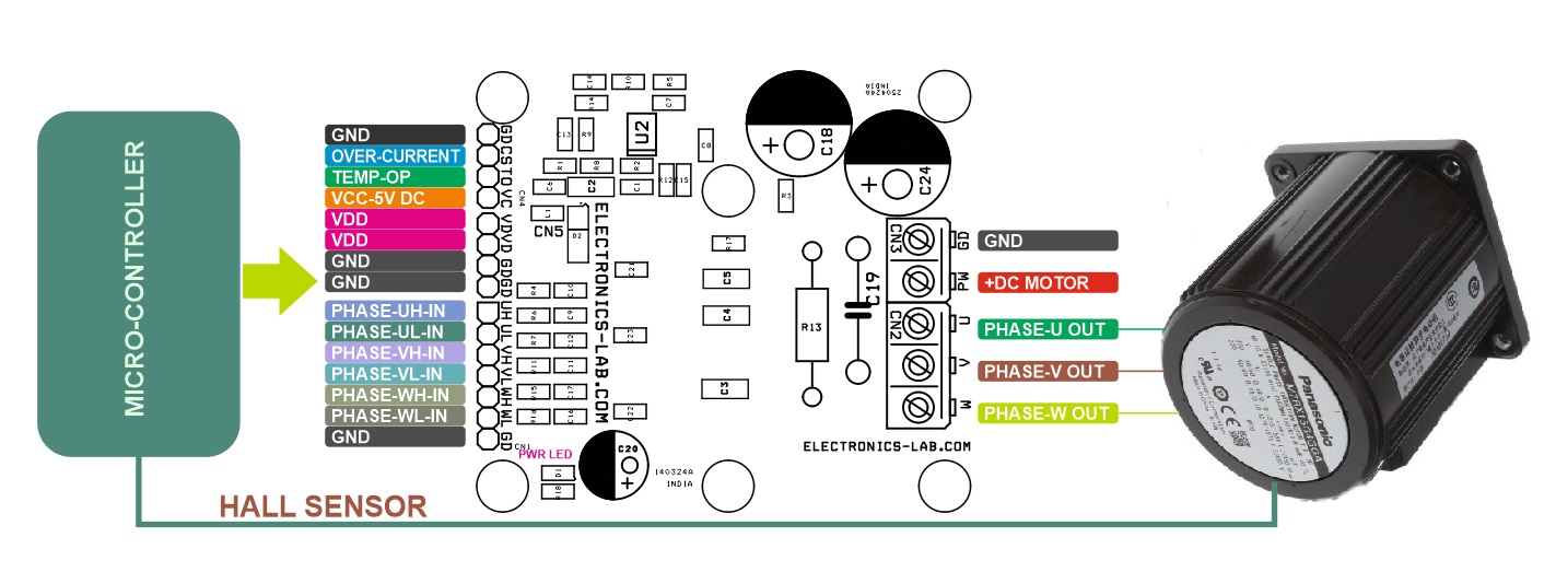
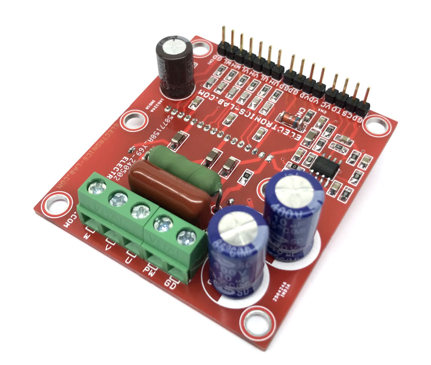
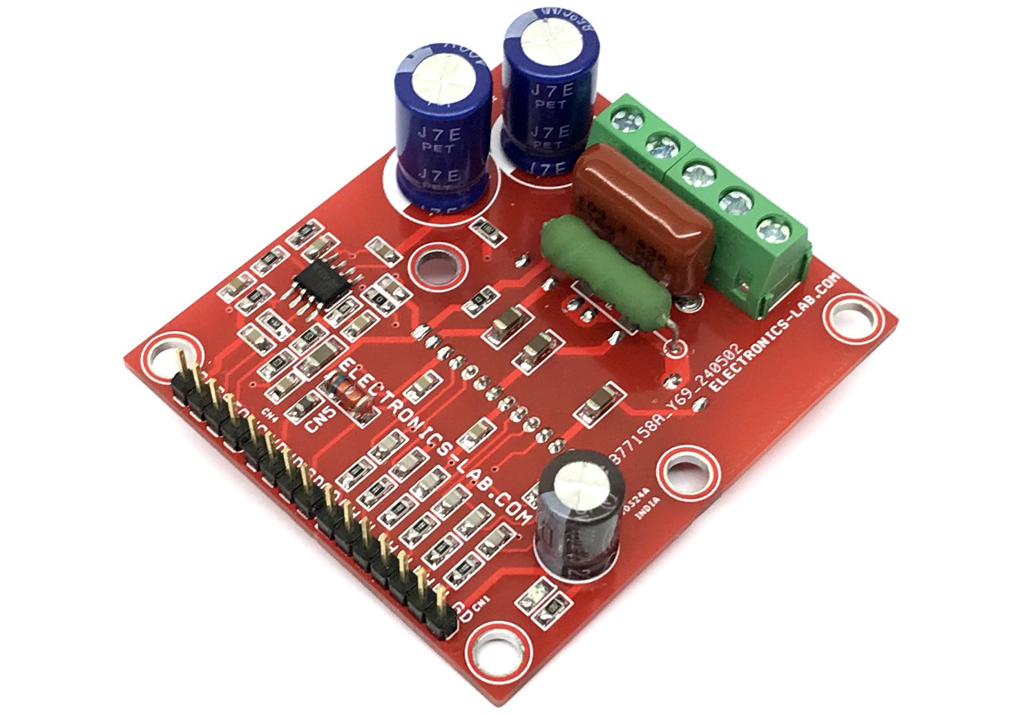
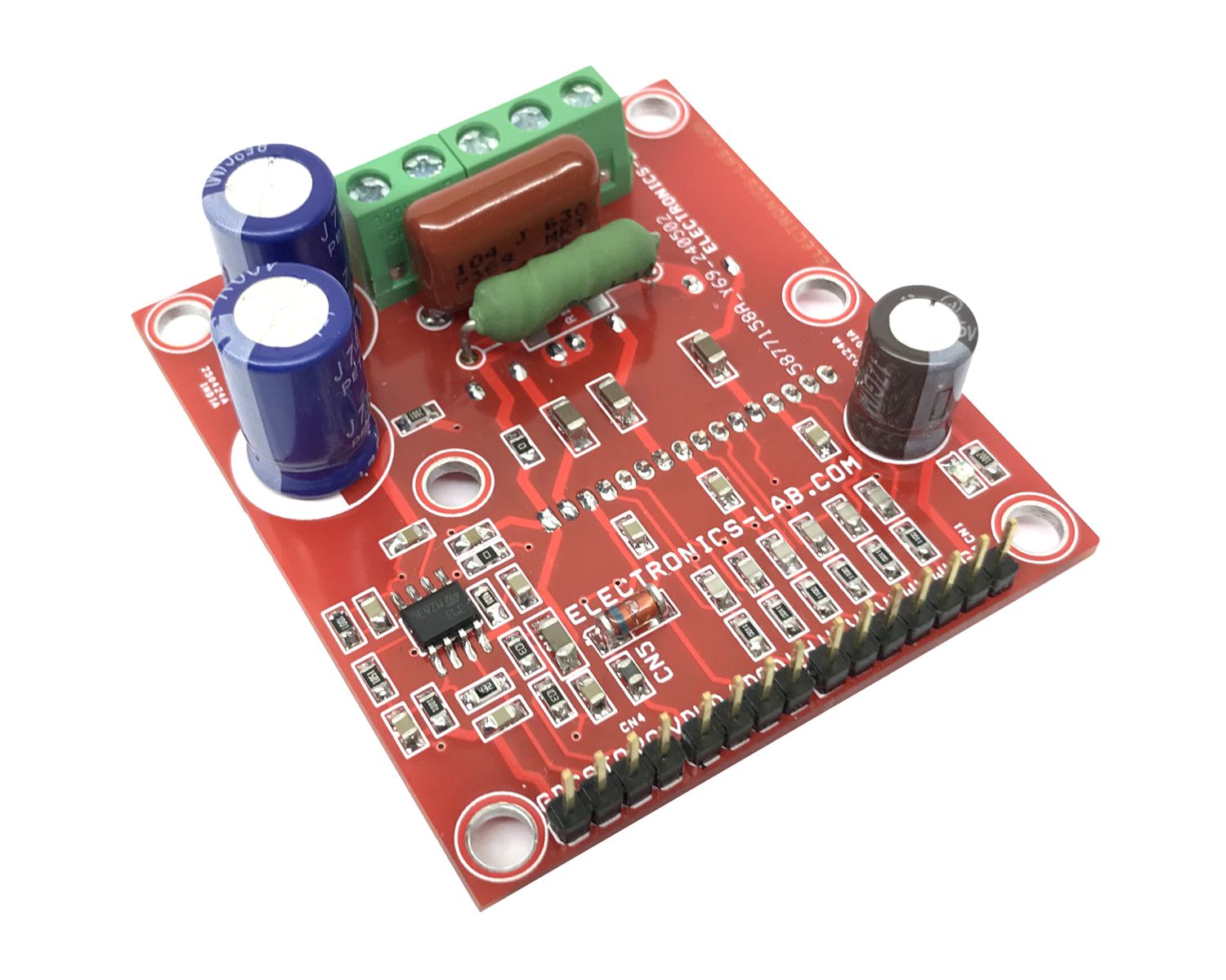
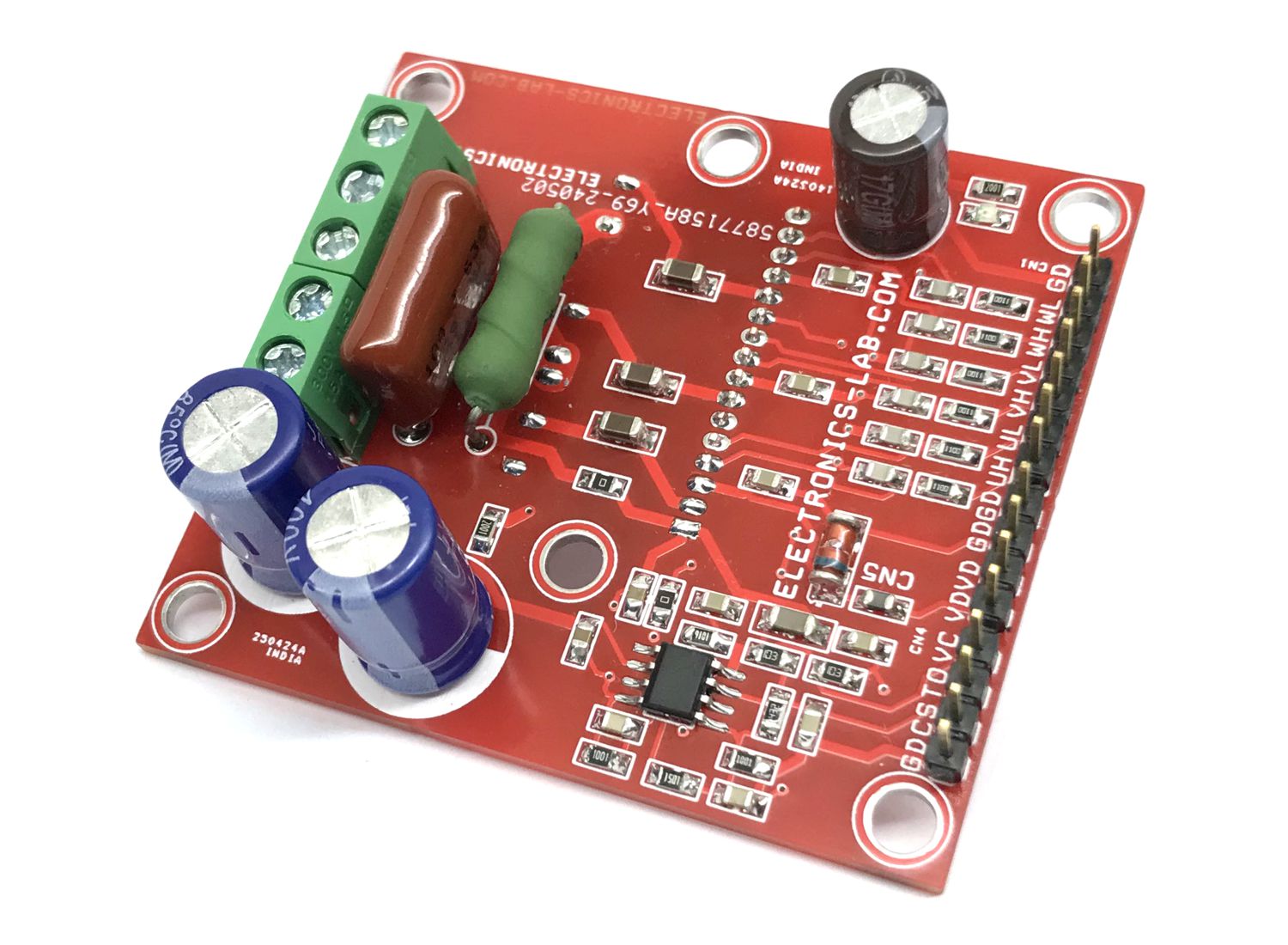
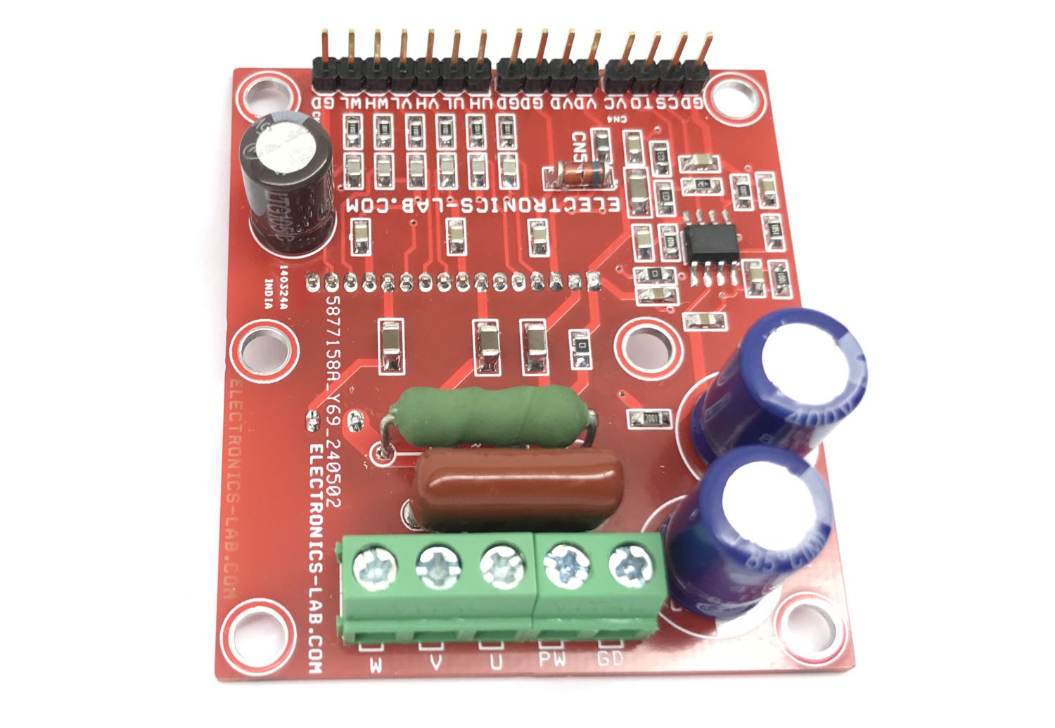
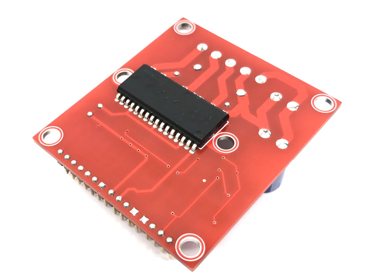
This is a Smart power module project designed for Small Power AC Motors. The FNB40560 chip is the heart of the project. A compact inverter project is ideal for small power motors such as fans and pumps. H-bridge configuration can also be created for low current high-voltage brushed DC motors. The Inverter project supports loads up to 5A. The DC power supply voltage is up to 400VDC. The project operates with 6 PWM signals. The parameters for bootstrap circuit elements are dependent on the PWM algorithm. For 5 kHz of switching frequency Bootstrap capacitors C2, C6, and C8 value is 33uF. Resistor R4, R5, R6, R12, R11, R8 and capacitor C9, C10, C11, C15, C16, C17 prevent improper signal due to surge-noise. ATS pin is provided to monitor the temperature of the IPM. A heatsink is needed for the IPM chip during operation or testing.
Note: The project operates with lethal voltage, user must take care of safety and all necessary precautions before testing the project.
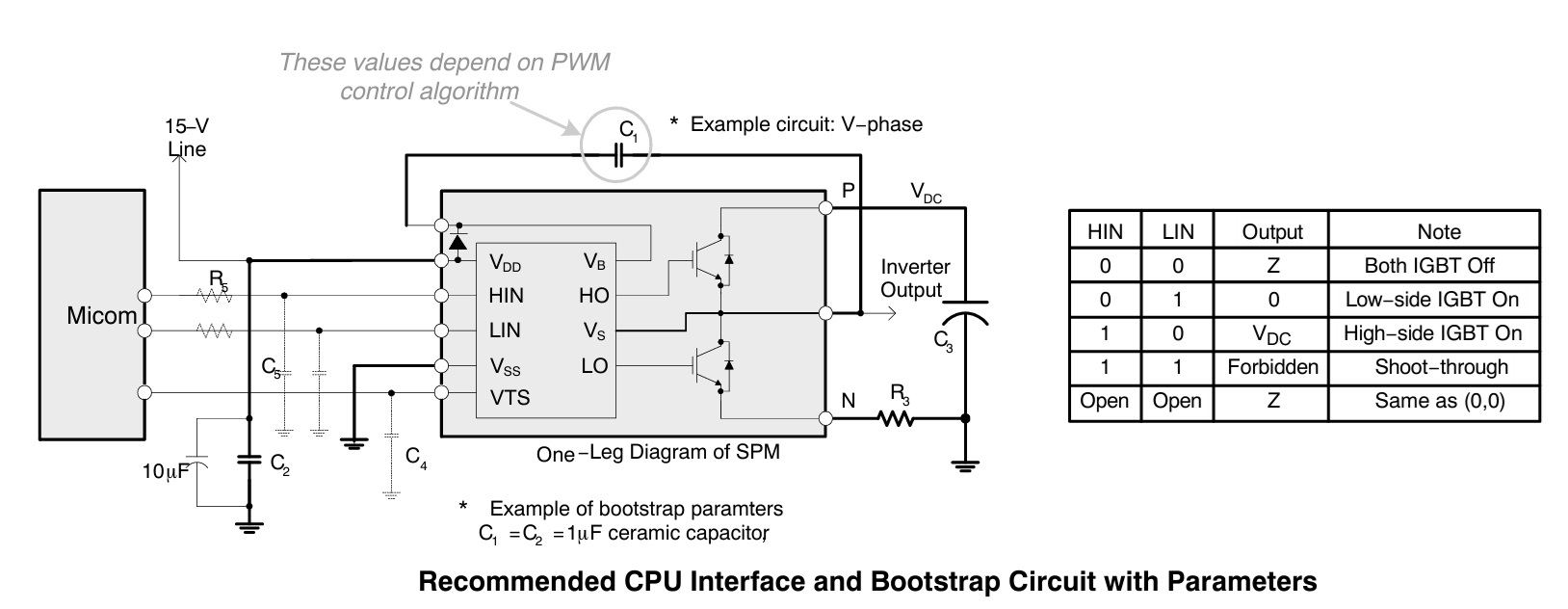
Operation Truth Table
HIN 0, LIN 0 = Output Z Both MOSFET Off
HIN 0, LIN 1 = Output 0 Low Side MOSFET On
HIN 1, LIN 0 = Output VDC High Side MOSFET On
HIN 1, LIN 1 = Forbidden Shoot Through
Features
Load Power Supply Up to 400V DC -+DC
Load Current Continues 5A
Logic Supply 15V DC (Gate Driver Circuit)-VDD
Power Supply for Temperature sense Circuit 5V DC-VCC
SCP, Over Current Trip Level 0.5V
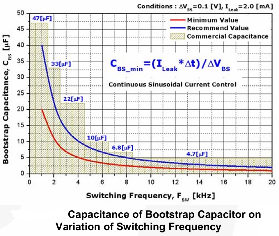
Input Frequency up to 20Khz (Choose Right Bootstrap Capacitor)
Power Supply for Over Current Circuit (Comparator CN5) 5V DC
One Board Power LED for Logic Supply
Shunt Based Over Current Feedback Output
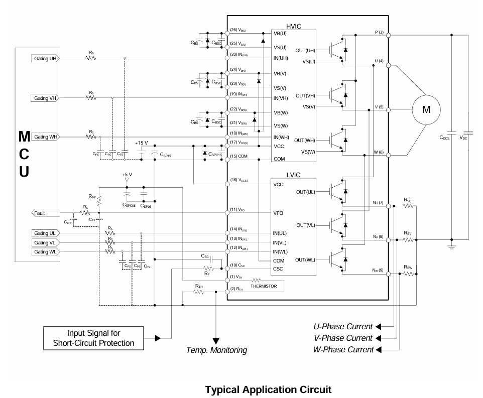
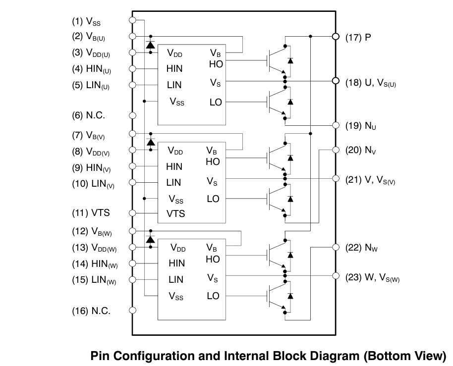
HVIC for gate driving and under-voltage protection
Active-High interface, can work with 3.3V/5V logic (PWM Signals)
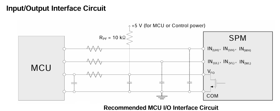
These pins are activated by voltage input signals. The terminals are internally connected to the Schmitt trigger circuit.
The signal logic of these pins is active HIGH; the MOSFET turns ON when sufficient logic voltage is applied to the associated input pin.
The wiring of each input needs to be short to protect the module against noise influences.
An RC filter is used to mitigate signal oscillations or any noise that traces of input signals may pick up.
Current Sense Resistor (Board provided with dual type of current sense resistor SMD or THT)
SMD 2512 Size 2 x Parallel Resistor
THT Solder Resistor
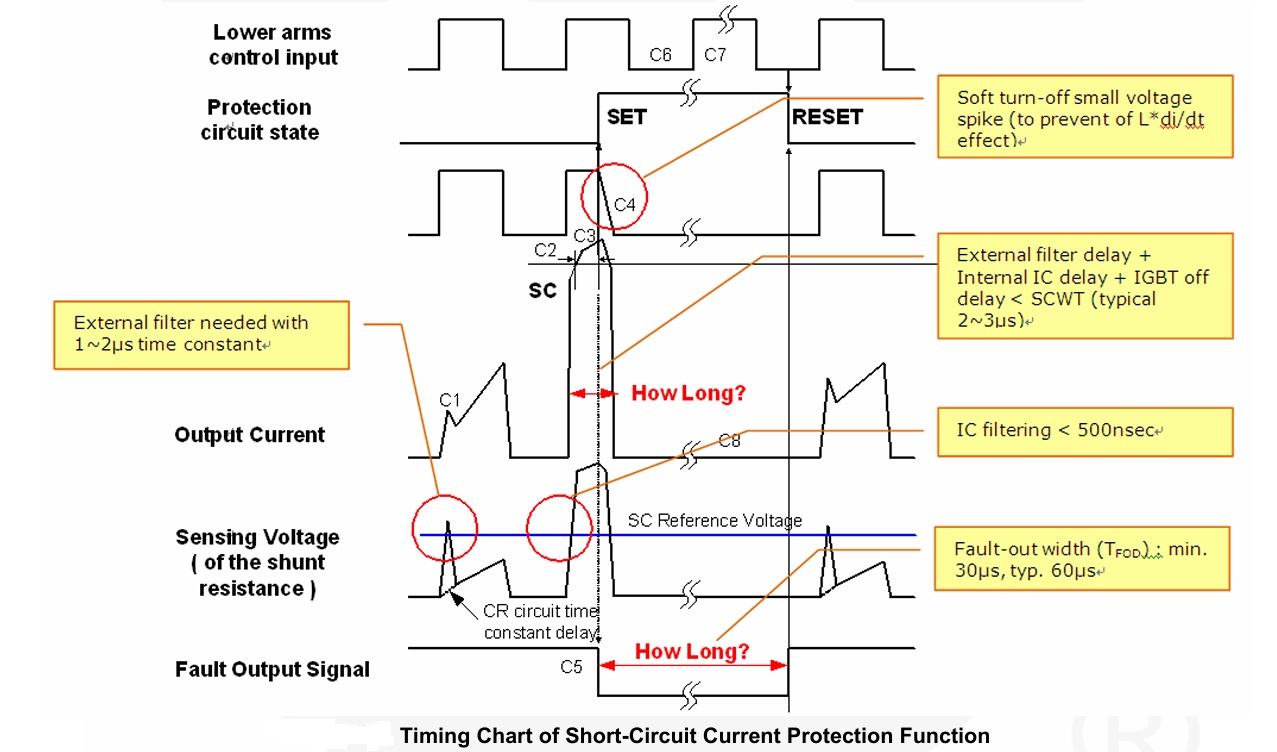
Short-Circuit Current Detection Pins
Pin: CSC
The current-sensing shunt resistor connected between the low-pass filter before the pin CSC and the low-side ground COM to detect short-circuit current
The shunt resistor should be selected to meet the detection levels matched for the specific application. An RC filter R7 and C14 connected to the CSC pin to eliminate noise. Connector CN5 provided for current feedback output, connector is connected across the shunt resistor. Refer Data sheet of IPM for more about trip voltage and shunt resistor.
Fault Output Pin (VFO)
The VFO output is open-drain configured. The VFO signal line is pulled up to the 5V logic power supply with approximately 4.7kΩ resistance.
This is the fault output alarm pin. An active LOW output is given on this pin for a fault state condition in the SPM.
The alarmed conditions are SCP (Short-Circuit Current Protection) or low-side bias UVLO (Under Voltage Lockout) operation.
Bootstrap Capacitor, C2, C6, C8
Value of bootstrap capacitor is depended on input frequency, refer the figure Bootstrap Capacitor VS frequency for capacitor selection, also refer data sheet for more info.
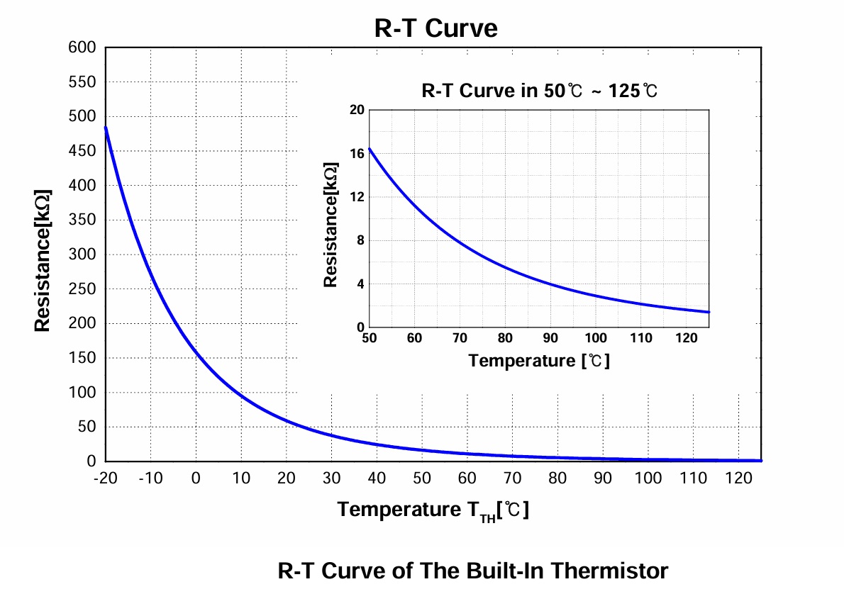
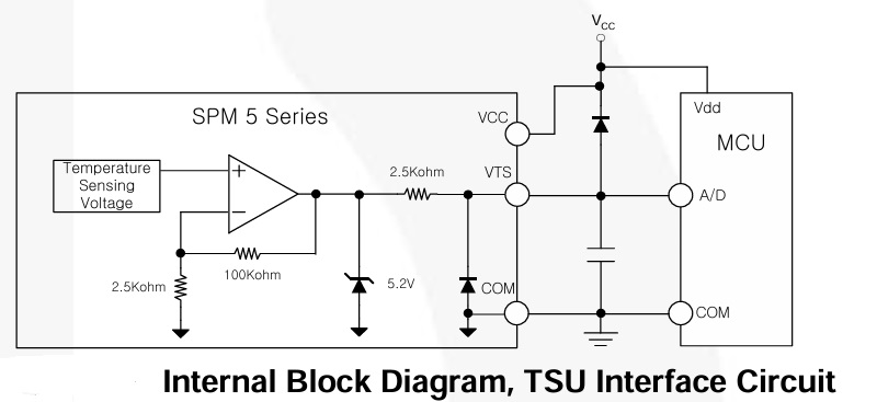
Thermistor Bias Voltage
Pin: VTH
This is the bias voltage pin of the internal thermistor. It is connected to the 5V logic power supply. Series Resistor for the Use of Thermistor (Temperature Detection)
Pin: RTH
For case temperature (TC) detection, this pin connected to an external series resistor R1. Temperature feedback output is available CN6 pin 2.
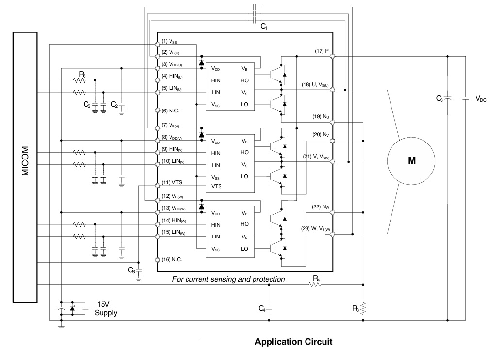
FNB40560 is a Motion SPM® 45 series that ON Semiconductor has newly developed to provide a very compact and high-performance inverter solution for AC motor drives in low-power applications such as refrigerators and dish washers. It combines low-loss short-circuit rated IGBTs and optimized gate drivers in a fully isolated package to deliver a simple and robust design. The system reliability is further enhanced by the built-in NTC for temperature monitoring, integrated under-voltage lock-out function for both high and low side, and an over-current protection input. Three separate open-emitter pins for low side IGBTs make three leg current sensing possible. Built-in bootstrap diodes and dedicated VS pins make PCB layout easy.
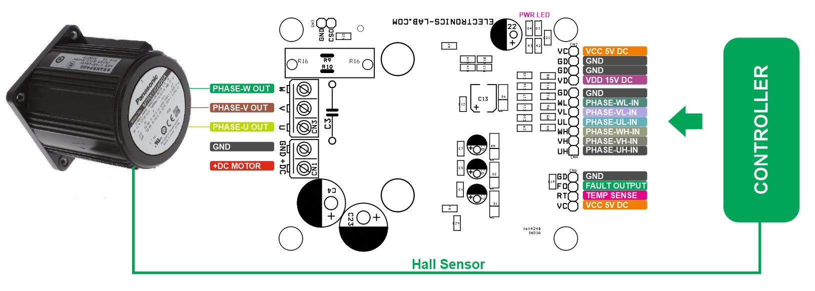
Connections
CN1: Pin 1 +DC Motor Power Supply up to 400V DC, Pin 2 = GND
CN2: Pin 1 15V DC for Logic Gate Driver, Pin 2 GND, Pin 3 = GND, Pin 4 = VCC 5V DC for Temperature Sensor
CN3: Pin 1 = Motor Phase U, Pin 2 = Motor Phase V, Pin 3 = Motor Phase W
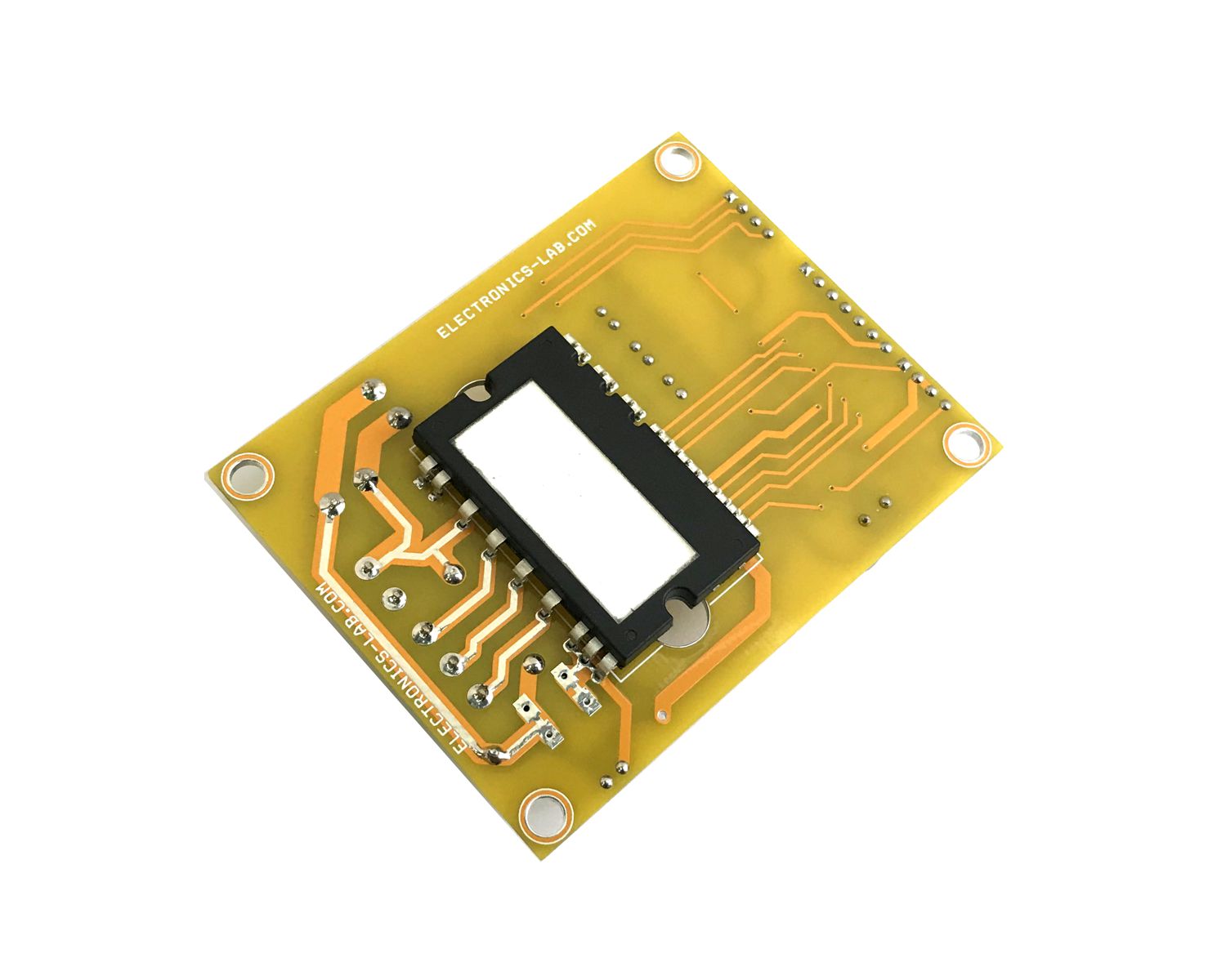
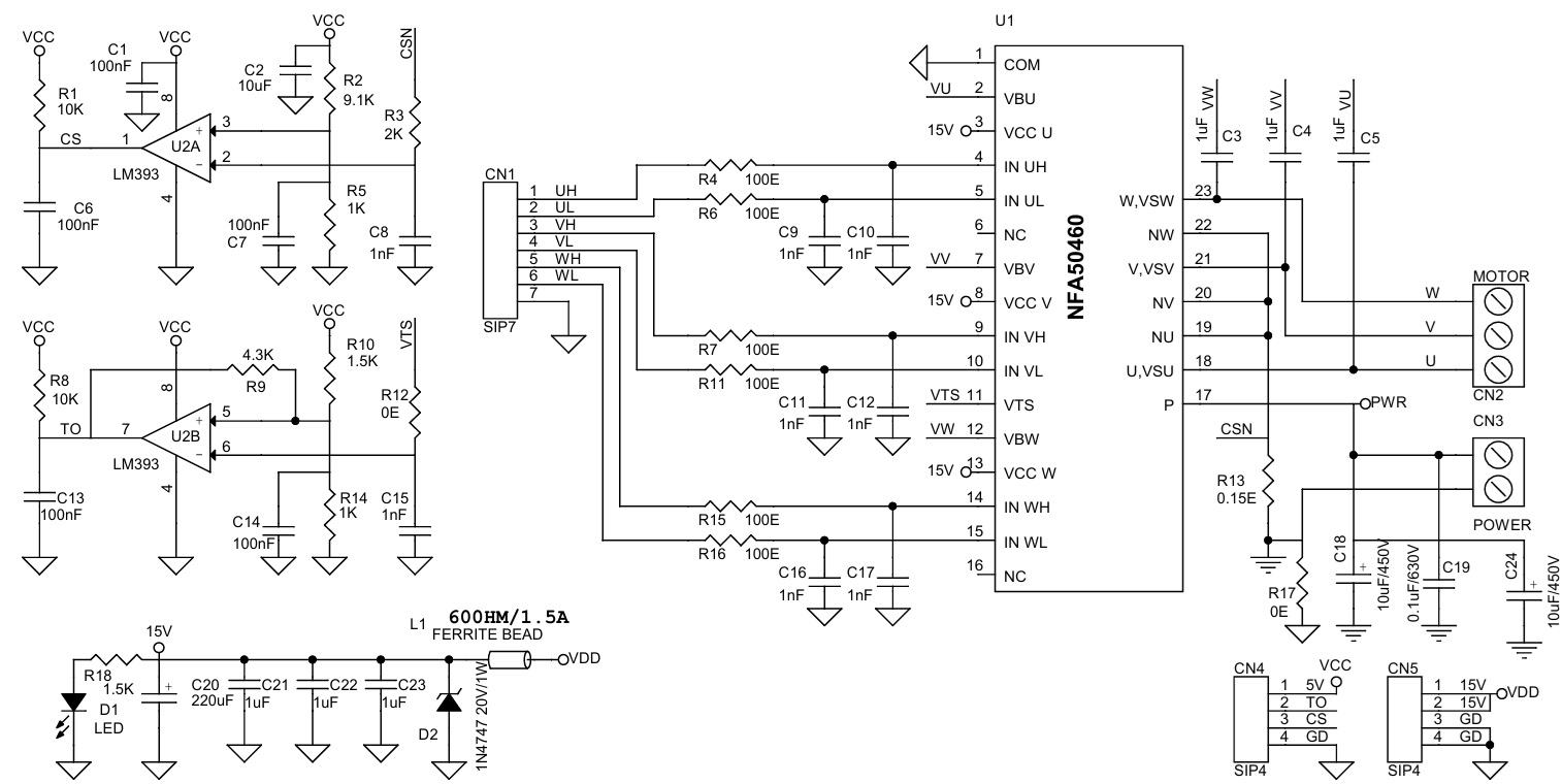
This is an advanced Motion module providing a fully featured, high-performance inverter output stage for AC induction, BLDC and PMSM motors such as refrigerators, fans, and pumps. This module is based on NFA50460 chip which integrates the optimized gate drive of the built−in IGBTs (FS4 RC IGBT technology) to minimize EMI and losses, while also providing multiple on−module protection features including under−voltage lockouts and thermal monitoring. The built−in high-speed Driver IC requires only a single supply voltage and translates the incoming logic−level gate inputs to the high voltage, high current drive signals required to properly drive the module’s internal IGBTs. Separate open emitter IGBT terminals are available for each phase to support the widest variety of control algorithms. Heatsink is a must for the IC before conducting any test.
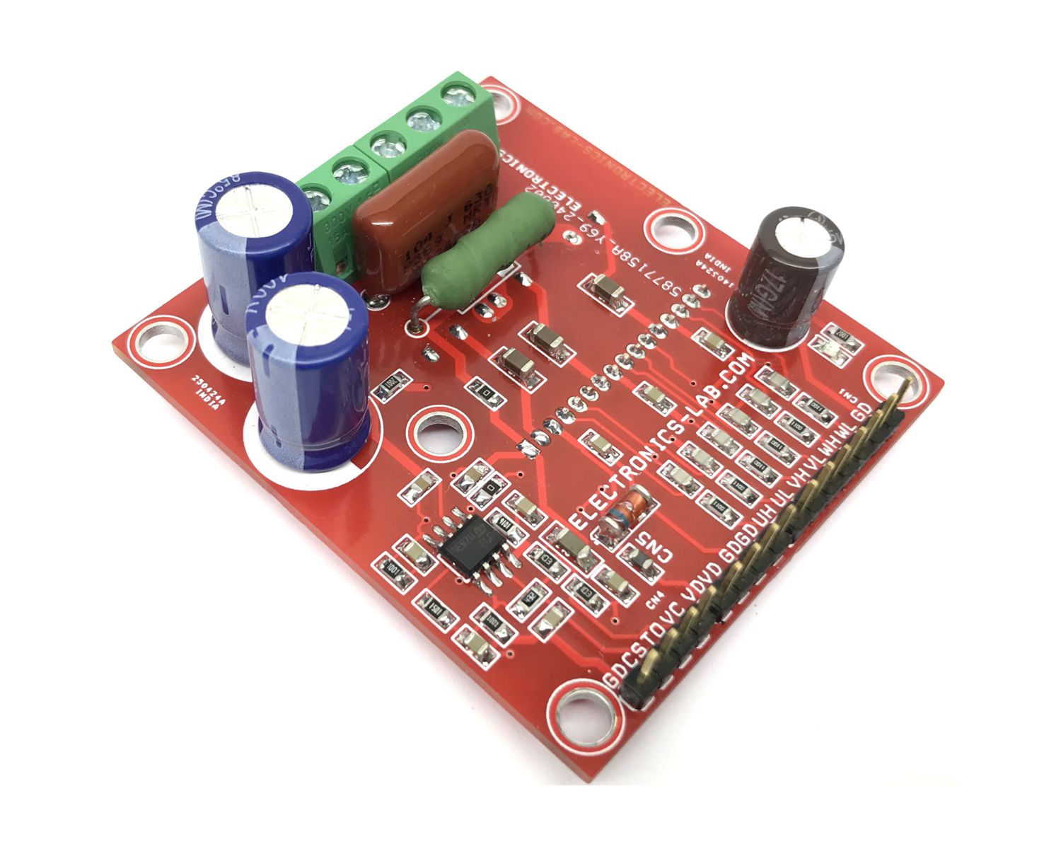
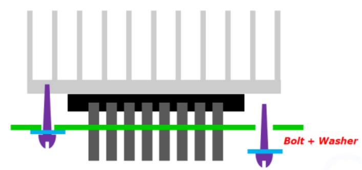
The project is built using NFA50460R4B IPM chip. This compact and reliable inverter project is ideal for small power motors such as fans and pumps. H-bridge configuration can also be created for low current high-voltage brushed DC motors. The Inverter project supports loads up to 4A. DC power supply voltage is up to 400VDC. The project operates with 6 PWM signals. Parameters for bootstrap circuit elements are dependent on PWM algorithm. For 15 kHz of switching frequency Bootstrap capacitors C3, C4, and C5 values is 1uF. Resistor R4, R6, R7, R11, R15, R16 and capacitor C9, C10, C11, C12, C16, C17 prevent improper signal due to surge-noise. The logic supply is protected with a 20V Zener diode, which prevents surge destruction under severe conditions. Comparator U2A provides low output when an over condition occurs, it measures the current across shunt resistor R13, and normally output is high. Comparator U2B is provided for over temperature, the output of U2B is high when IPM temperature is below 80 degrees C and goes low when the temperature reaches the threshold. A heatsink is a must for full load current, 2 mounting holes are provided throughout the PCB to mount the heatsink as shown in Figure below. Silicone thermal compound, also called thermal grease, should be applied between the heat sink and the flat surface of the IPM to fill microscopic air gaps due to imperfect flatness that ultimately reduces the contact thermal resistance. The IPM module should be soldered first. Excessive torque may bend the PCB.
Note 1: The project operates with lethal voltage and the user must take care of safety and all necessary precautions before testing the project.
Note 2: The board has dual option current sense resistor R13. The resistor must be 1% THT or SMD size 2512.
Features
Load Power Supply Up to 400V DC (Maximum 450V DC)
Load Current Continues 4A
Logic Supply 15V DC, Current 100mA
Power Supply for Over Current/Temperature Circuit (Comparator U2) 5V DC
One Board Power LED for Logic Supply
Shunt and Comparator Based Over Current Output
Over temperature threshold is 80 degrees centigrade.
HVIC for gate driving and under-voltage protection
Active-High interface, can work with 3.3V/5V logic (PWM Signals)
On Threshold Voltage 2.9V, Off Threshold Voltage 0.8V
Optimized for low electromagnetic interference
Isolation voltage rating of 1500Vrms for 1min
4 x 4 mm Mounting Holes
PCB Dimensions 60.64 x 54.29 mm
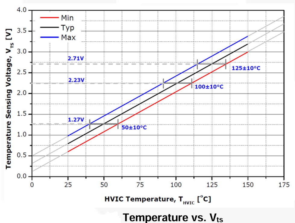
Temperature Sensing Output (VTS) – CN4 Pin 2-TO
Pin: VTS This indicates the temperature of the V-phase HVIC with analog voltage. HVIC itself creates some power loss, but mainly heat generated from the MOSFETs increases the temperature of the HVIC. Comparator U2B is used for over temperature. Output is high in normal condition when temperature is below 80 degrees, goes low when over temperature condition occurs. Over temperature threshold is 80 degrees centigrade.
Current Sense
Current sense resistor R13, Comparator U2A provided to sense the current, this circuit activates when over current condition occurs, output of U2A is normally high, goes low when over condition occurs. Threshold of over current can be alter using divider resistor R2 and R5.
These pins are activated by voltage input signals. The terminals are internally connected to the Schmitt trigger circuit.
The signal logic of these pins is active HIGH; the MOSFET turns ON when sufficient logic voltage is applied to the associated input pin.
The wiring of each input needs to be short to protect the module against noise influences.
An RC filter is used to mitigate signal oscillations or any noise that traces of input signals may pick up.
NFA50460R4B is an advanced Motion SPM 5 Series based on FS4 RC−IGBT technology as a compact inverter solution for small power motor drive applications such as fans and pumps. Embedded six FS4 RC−IGBTs, three half−bridge gate drive HVICs with temperature sensing, and three bootstrap diodes in a compact package fully isolated and optimized for thermal performance. Major features are low Electro−magnetic Interference (EMI) characteristics through optimizing switching speed and reducing parasitic inductance. Since IGBTs are employed as power switches, it provides much more ruggedness and larger Safe Operating Area (SOA) than IGBT based power modules. Right solution for compact and reliable inverter designs where the assembly space is constrained.
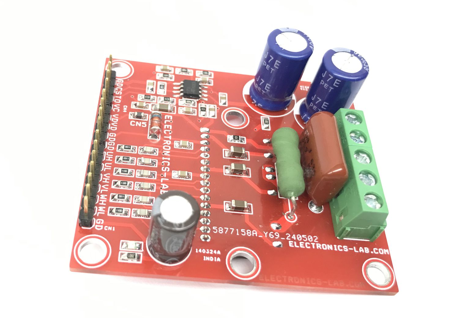
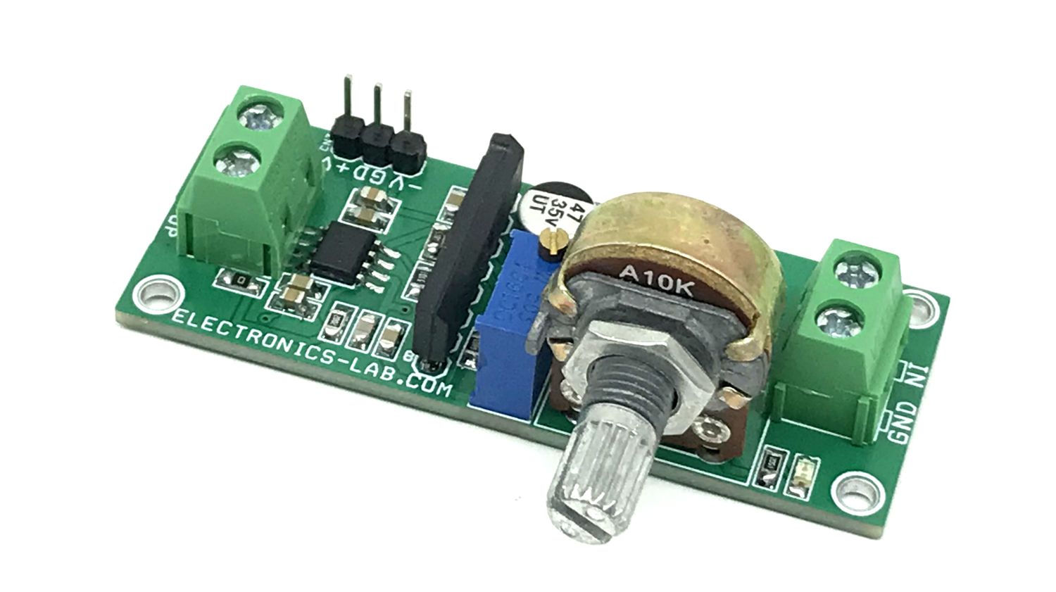
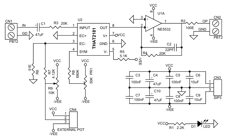
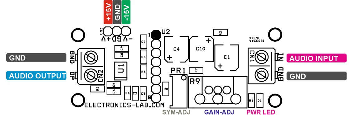
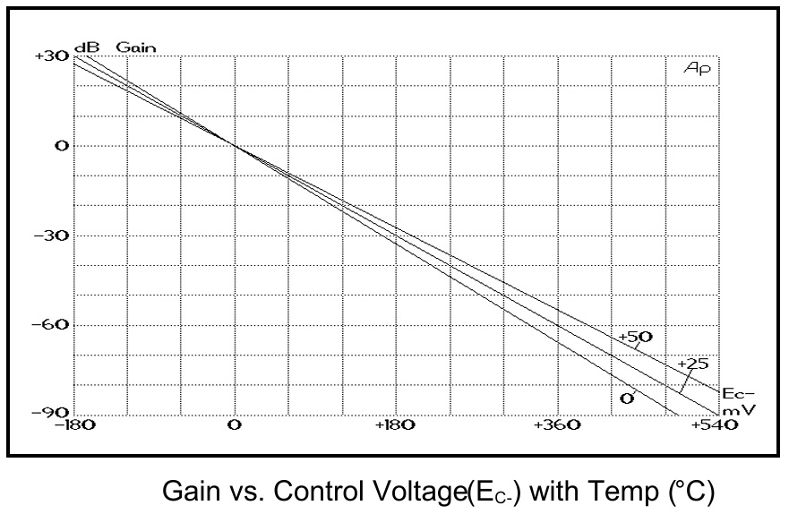
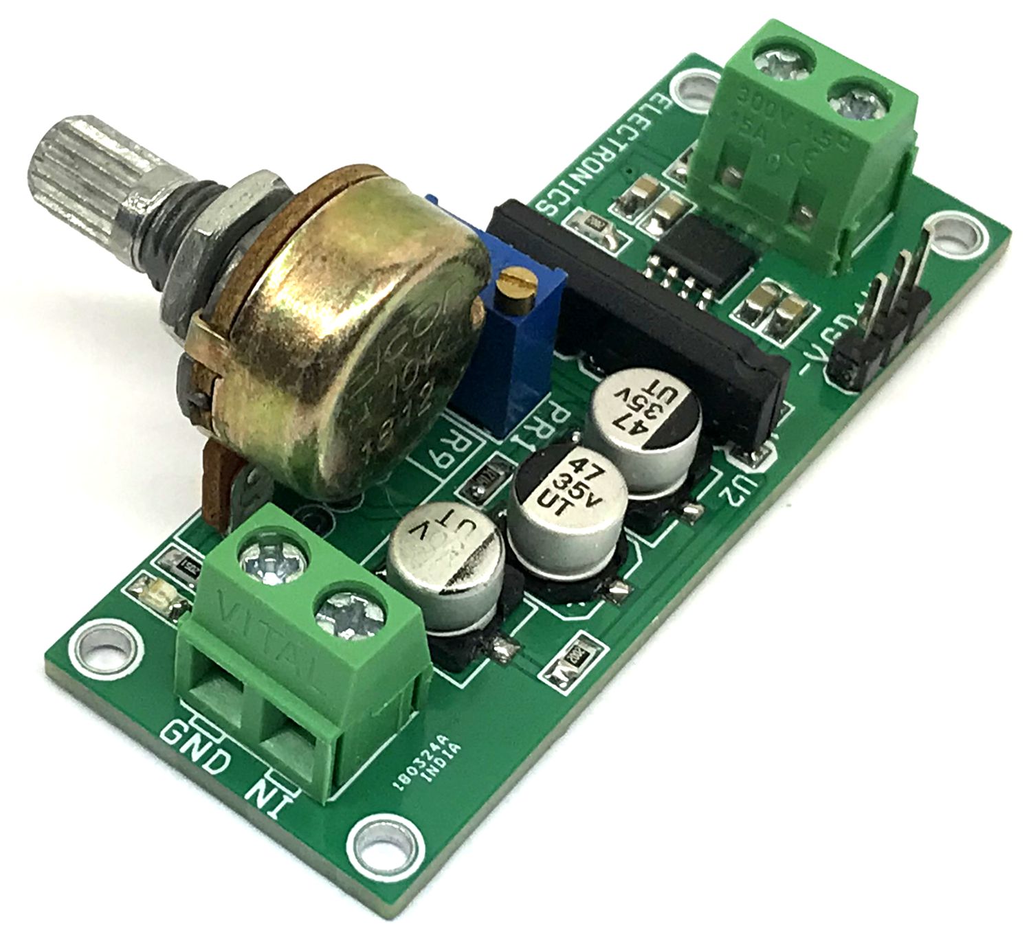
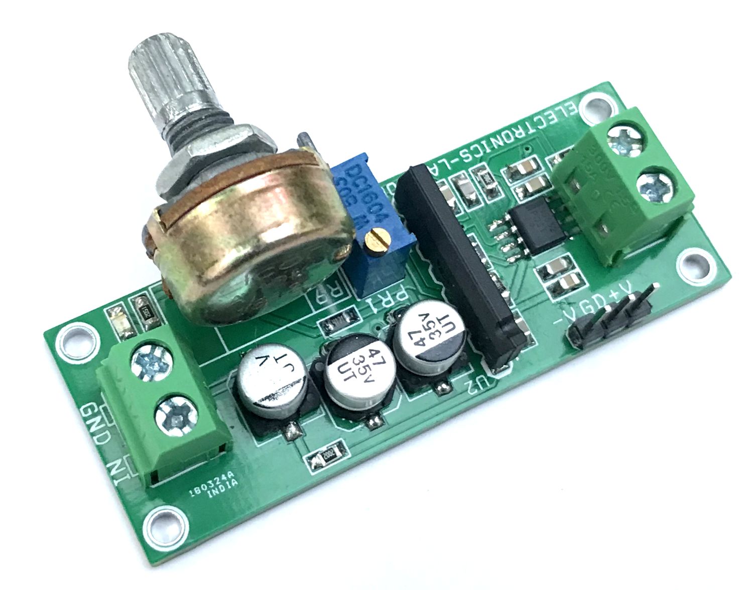
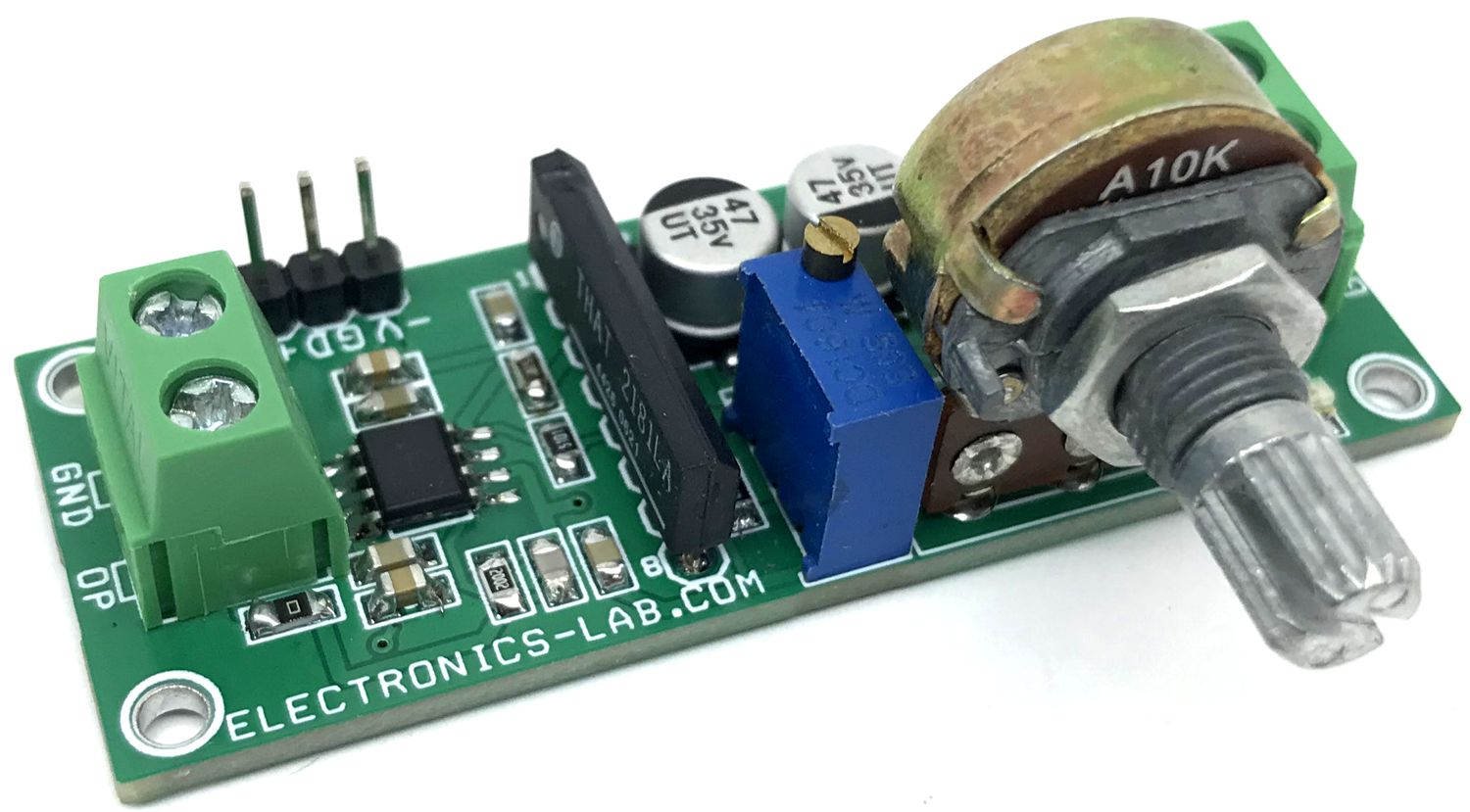
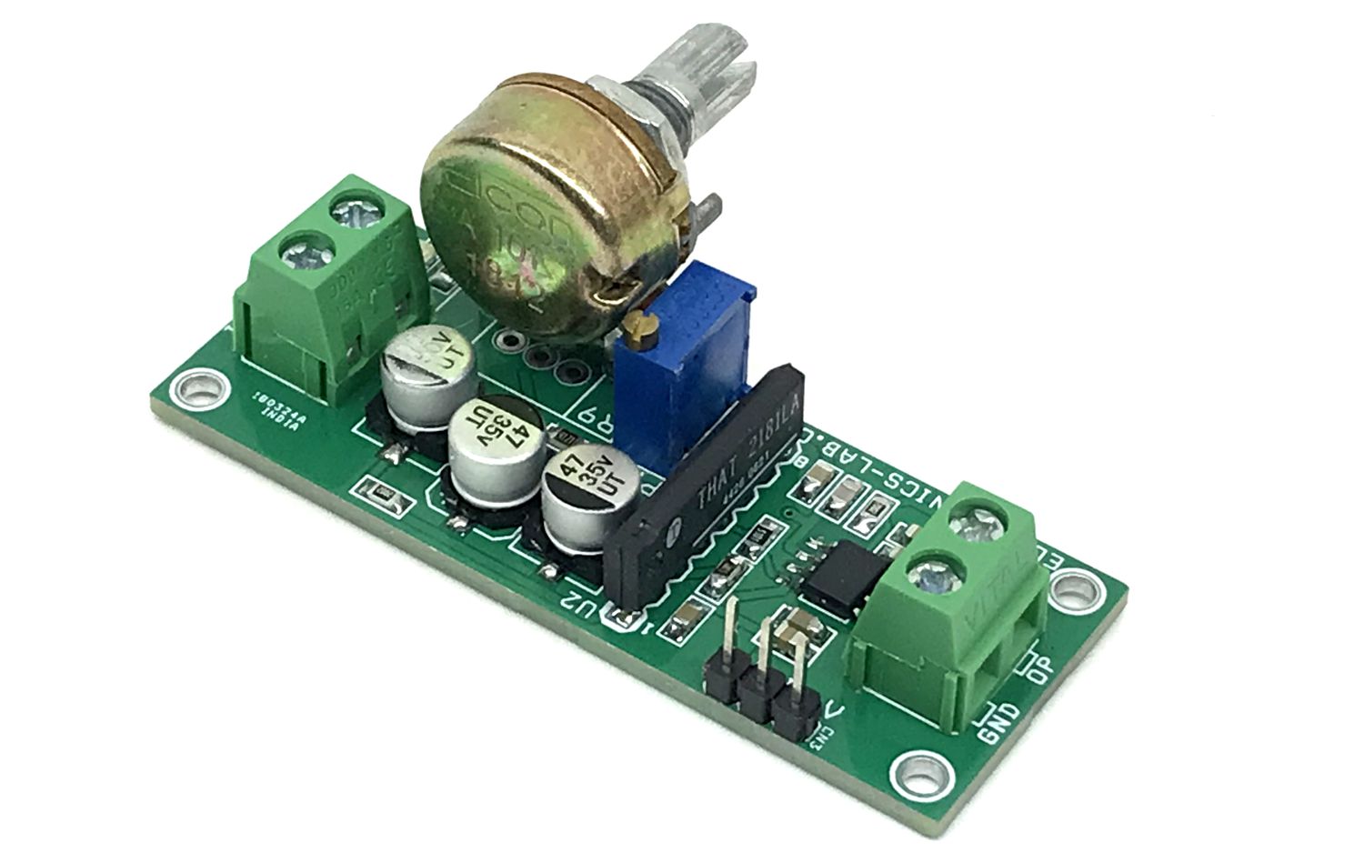
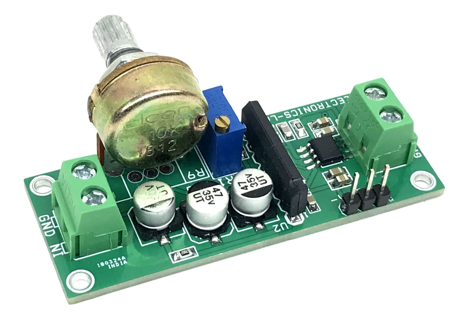
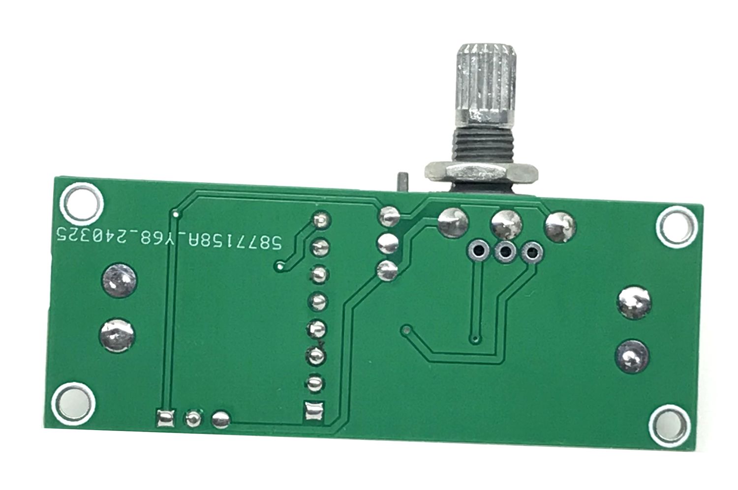
The project presented here is a Voltage Controlled Amplifier (VCA). A VCA board helps users control the Audio Level from a remote potentiometer. It requires a single-ended audio signal in the input. Gain control voltage can be adjusted through an on-board potentiometer or use an external potentiometer connected to CN4. The project works with a dual ±15V power supply. Screw terminal connectors are provided for signal input and signal output. The project is built using THAT2181LA chip, a VCA that is designed for high-performance audio-frequency applications requiring exponential gain control, low distortion, wide dynamic range, and low control-voltage feedthrough. These parts control gain by converting an input current signal to a bipolar logged voltage, adding a DC control voltage, and re-converting the summed voltage back to a current through a bipolar antilog circuit. Stereo control of VCA with a single potentiometer is possible.
THAT 2181-series trimmable Blackmer voltage-controlled amplifier (VCAs) ICs are very high-performance current-in/current-out devices with two opposing-polarity, voltage-sensitive control ports. They offer wide-range exponential control of gain and attenuation with low signal distortion.
Trimming
The trim should be adjusted for minimum harmonic distortion using PR1. This is usually done by applying a middle-level, middle-frequency signal (e.g. 1 kHz at 1 V) to the audio input, setting the VCA to 0 dB gain, and adjusting the SYM trim while observing THD at the output. In THAT2181LA, this adjustment coincides closely with the setting which produces minimum control-voltage feedthrough, though the two settings are not always identical.
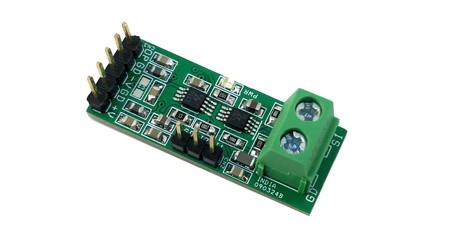
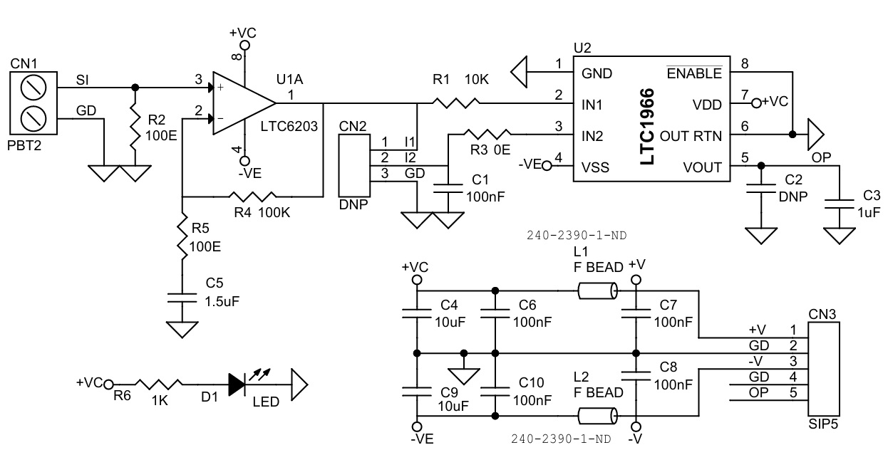
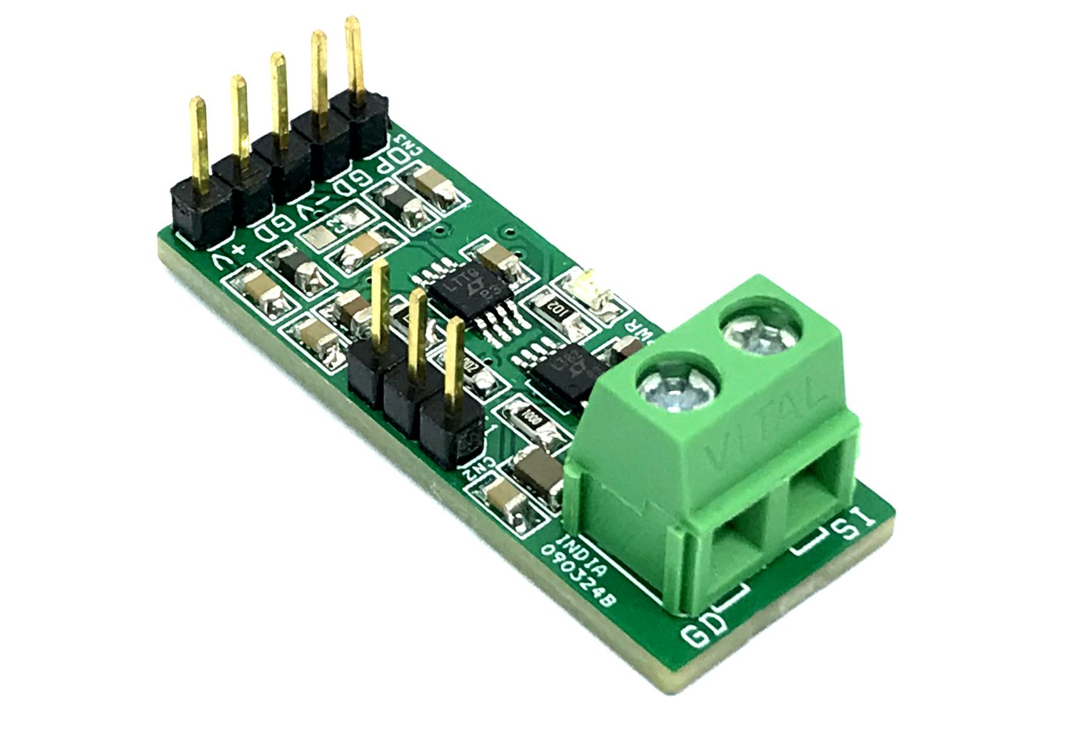
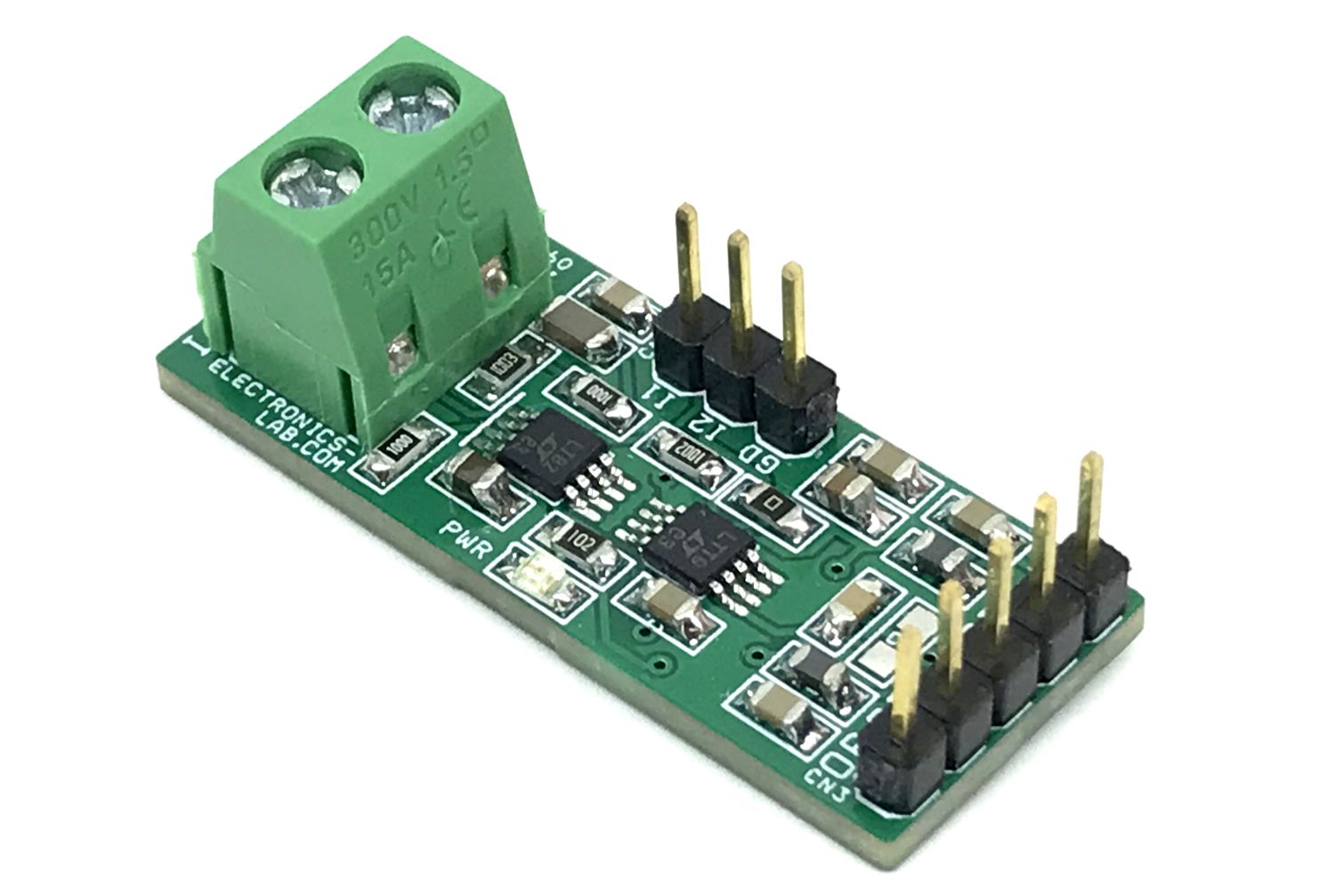
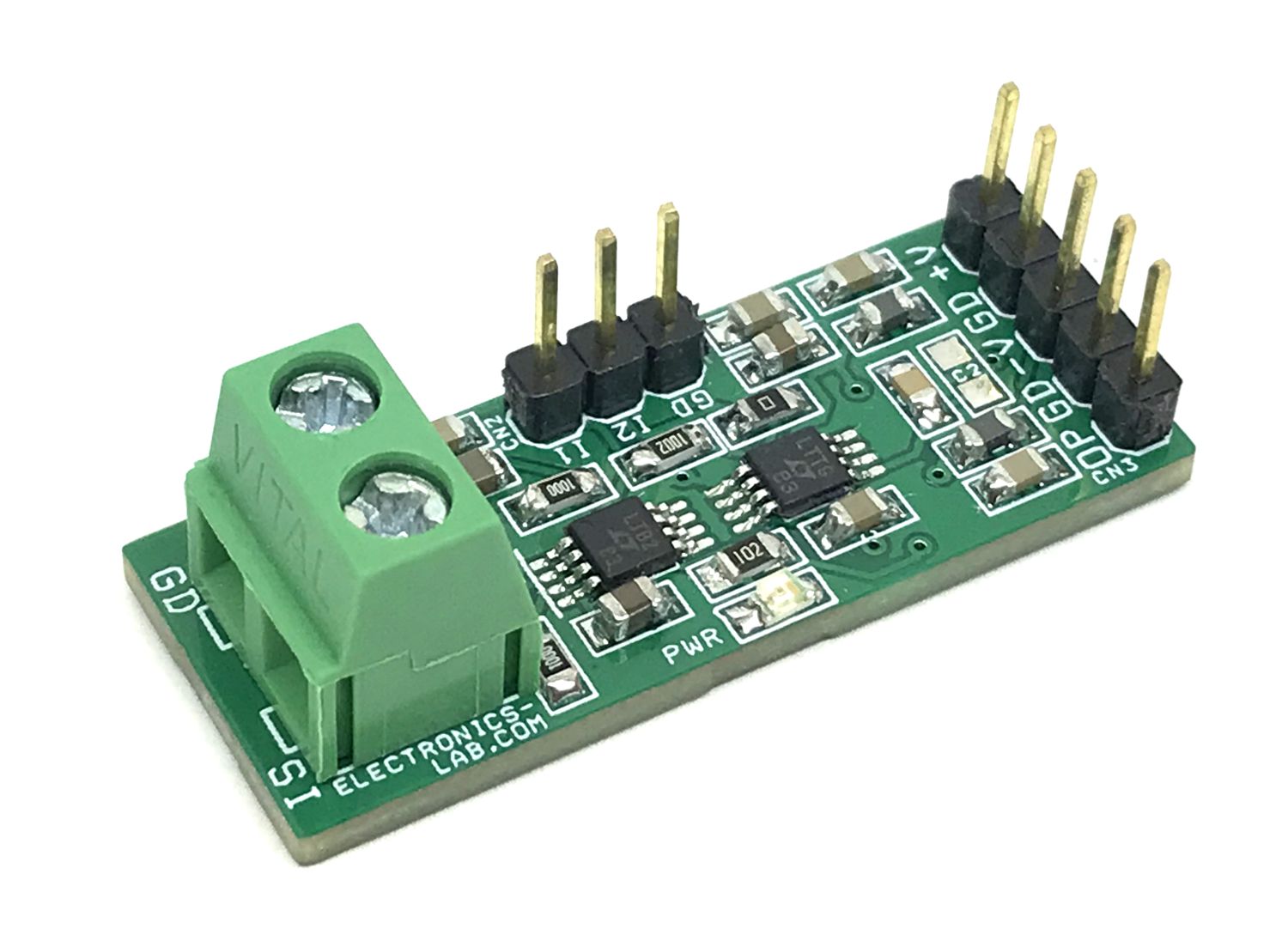
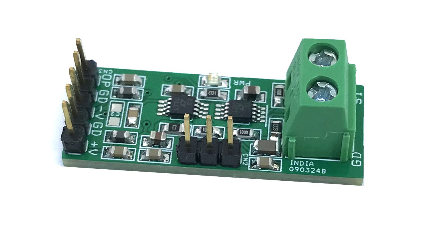
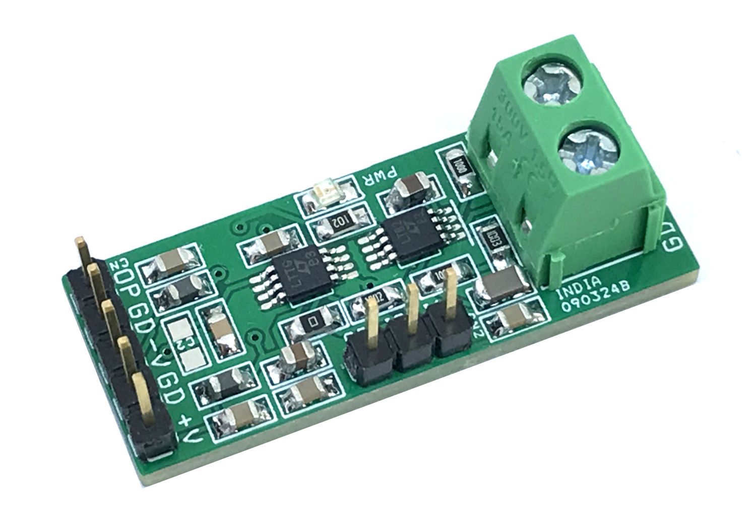
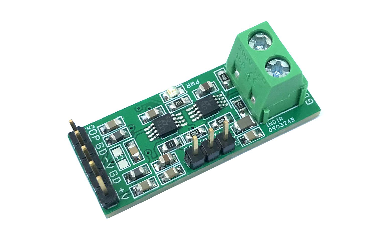
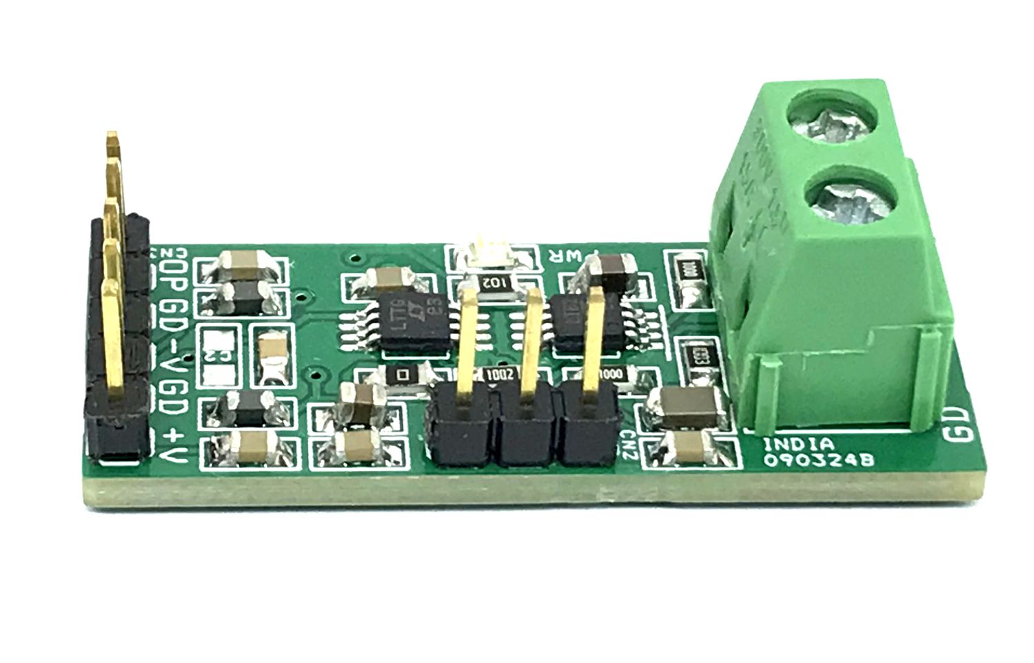
This mini-module helps users to measure the RMS noise of AC signal. Apply the AC noise signal to the input and the circuit outputs a DC voltage. Signal bandwidth is 1Khz to 100Khz and input sensitivity is 1 μVolt RMS. The LT6203 ultra-low noise, low power op-amp amplifies the low-level signal. Further, this signal is converted into a DC voltage by LTC1966 True RMS converter chip from Analog Devices. The circuit works with dual supply +/-5V DC and consumes very low current.
VOutput = 1mVDC/1μVolt RMS Noise
Credits: Schematic is from Analog Devices Application note.