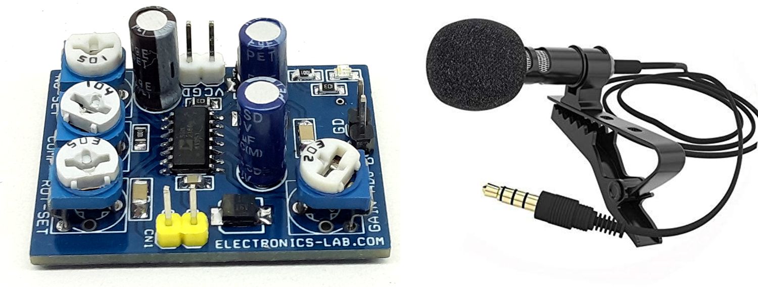
Hi-End Microphone Preamplifier with Variable Compression, Noise Gating and Adjustable Gain
The circuit shown here is a complete microphone signal conditioning system based on a single SSM2166 integrated circuit. Designed primarily for voiceband applications, this integrated circuit provides amplification, RMS detection, limiting, variable compression, and downward expansion.
The circuit shown here is a complete microphone signal conditioning system based on a single SSM2166 integrated circuit. Designed primarily for voiceband applications, this integrated circuit provides amplification, RMS detection, limiting, variable compression, and downward expansion. An integral voltage-controlled amplifier (VCA) provides up to 60dB of gain in the signal path with approximately 30kHz bandwidth. Additional gain is provided by an input buffer OPAMP circuit that can be set anywhere from 0 dB to 20 dB, for a total signal path gain of up to 80 dB. The project operates on a single +5 V supply, accepts input signals up to 1Vrms, and produces output signal levels > 1 Vrms (3Vp-p) into loads > 5 kΩ. The internal RMS detector has a time constant set by an external capacitor. The SSM2166 contains an input buffer and automatic gain control (AGC) circuit for audio and voiceband signals. Circuit operation is optimized by providing a user-adjustable time constant and compression ratio. A downward expansion (noise gating) feature eliminates circuit noise in the absence of an input signal. Onboard trimmer potentiometer allows the user to set the downward expansion threshold, the limiting threshold (rotation point), input buffer fixed gain, and the internal VCA’s nominal gain at the rotation point.
Features
- Operating Supply 5V DC (4.5V to 5.5V)
- Supports Condenser Microphone
- Adjustable Compressions Ration using Trimmer Potentiometer
- Adjustable Rotation Point using Trimmer Potentiometer
- Adjustable Noise Gate Threshold using Trimmer Potentiometer
- Header Connector for Microphone
- Header Connector for Output
- Header Connector for Supply input
- Low Noise and Distortion
- Power-Down Feature
- 20 kHz Bandwidth (61 dB)
- Power LED D1
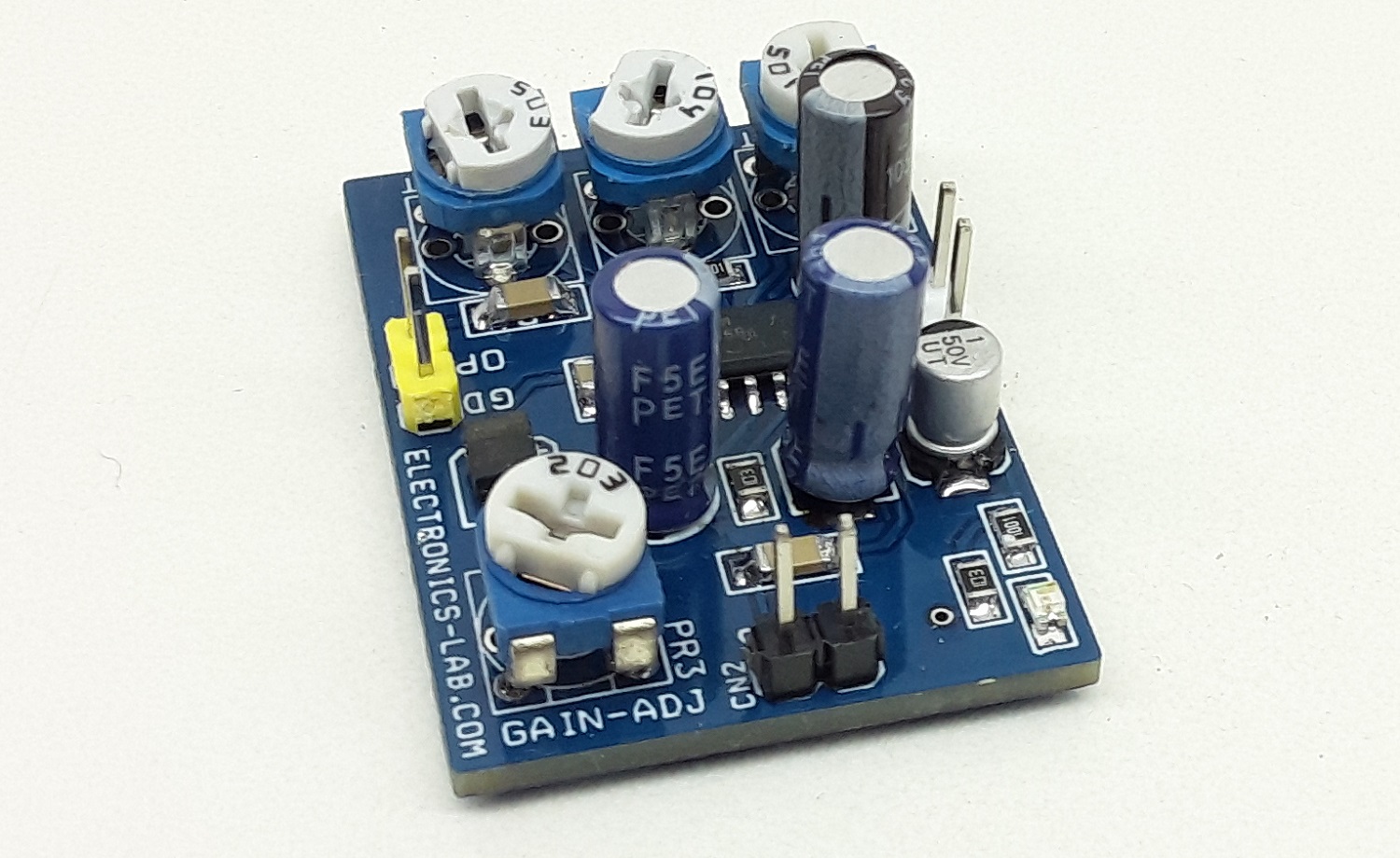
- PCB Dimensions 36.99 x 26.51 mm
Compression Ratio (Can be set Using Optional Fixed Resistor R9 or Trimmer Potentiometer PR4)
The compression ratio may be varied from 1:1 (no compression) to over 15:1 via a Trimmer potentiometer PR4 or Optional resistor R9, RCOMP. Input signals above VRP are compressed with a fixed compression ratio of approximately 15:1. The compression ratio can be set by adjustable trimmer Pot PR4 connected between the COMP RATIO pin (Pin 10) and GND or optional R9. Lowering RCOMP gives smaller compression ratios. with values of about 17 kΩ or less resulting in a compression ratio of 1:1. AGC performance is achieved with compression ratios between 2:1 and 15:1, and is dependent on the application. A 100 kΩ potentiometer PR4 used to allow this parameter to be adjusted.
This region of operation is the “limiting region.” Varying the compression ratio has no effect on the limiting region. The breakpoint between the compression region and the limiting region is referred to as the “limiting threshold” or the “rotation point,” and is user-specified in the SSM2166. The term “rotation point” derives from the observation that the straight line in the compression region “rotates” about this point on the input/output characteristic as the compression ratio is change
Gain Adjust -Trimmer Potentiometer PR3 or Optional Resistor R3
The maximum gain of the project is set by the GAIN ADJUST Trimmer pot PR3. This resistor, with a range between 1 kΩ and 20 kΩ, will cause the nominal VCA gain to vary from 0 dB to approximately 20 dB, respectively. To set the VCA gain to its maximum can also be achieved by leaving the GAIN ADJUST pin in an OPEN condition (no connect).
The gain of the system with an input signal level of VRP is fixed by RGAIN regardless of the compression ratio, and is the “nominal gain” of the system. The nominal gain of the system may be increased by the user via the onboard VCA by up to 20 dB. Additionally, the input buffer of the SSM2166 is configured to provide fixed gains of 0 dB to 20 dB with R2 and R4. The gain of the VCA at the rotation point is set by the value of an optional resistor R3 or trimmer potentiometer PR3 connected between Pin 2 and GND, RGAIN.
Rotation Point Adjustment – Trimmer Potentiometer PR1 or Optional Resistor R6
Rotation Point. An internal dc reference voltage in the control circuitry, used to set the rotation point. By varying a trimmer potentiometer PR1 or optional resistor R6, connected between the positive supply and the ROTATION POINT SET pin (Pin 11), the rotation point may be varied from approximately 20 mV rms to 1 V rms. From the figure, the rotation point is inversely proportional to RROT PT. For example, a 1 kΩ resistor would typically set the rotation point at 1 V rms, whereas a 55 kΩ resistor would typically set the rotation point at approximately 30 mV rms. Since limiting occurs for signals larger than the rotation point (VIN > VRP), the rotation point effectively sets the maximum output signal level. It is recommended that the rotation point be set at the upper extreme of the range of typical input signals so that the compression region will cover the entire desired input signal range. Occasional larger signal transients will then be attenuated by the action of the limiter.
Noise Gate Adjust – Trimmer Potentiometer PR2 or Optional Resistor R7
The range of the noise gate is from 0.3 mV to over 0.5 mV relative to the output of the buffer. To fit this range to your application, you may have to attenuate the input or apportion the buffer gain and VCA gain differently.
Operations
The audio input signal is processed by the input buffer and then by the VCA. The input buffer presents an input impedance of approximately 180 kΩ to the source. A dc voltage of approximately 1.5 V is present at AUDIO +IN (Pin 7 of the SSM2166), C4 provided as a blocking capacitor for ground-referenced sources. A 0.1 µF capacitor is a good choice for most audio applications. The input buffer is a unity-gain stable amplifier that can drive the low impedance input of the VCA. The VCA is a low distortion, variable-gain amplifier whose gain is set by the side-chain control circuitry. The input to the VCA is a virtual ground in series with approximately 1 kΩ. Capacitor C3 provided for blocking purpose between the buffer’s output and the VCA input. The 1 kΩ impedance between amplifiers determines the value of this capacitor which is typically between 10 µF. The VCA amplifies the input signal current flowing through C3 and converts this current to a voltage at the SSM2166’s output pin (Pin 13). The net gain from input to output can be as high as 60 dB (without additional buffer gain), depending on the gain set by the control circuitry.
The gain of the VCA at the rotation point is set by the value of a resistor connected between Pin 2 and GND, RGAIN. The AGC range of the SSM2166 can be as high as 60 dB. The VCAIN pin (Pin 3) on the SSM2166 is the noninverting input terminal to the VCA. The output impedance of the SSM2166 is typically less than 75 Ω, and the external load on Pin 13 should be >5 kΩ. The nominal output dc voltage of the device is approximately 2.2 V. Capacitor C8 provided on output for blocking purpose for grounded loads. The bandwidth of the SSM2166 is quite wide at all gain settings. The upper 3 dB point is approximately 30 kHz at gains as high as 60 dB (using the input buffer for additional gain, circuit bandwidth is unaffected). The lower 3 dB cut-off frequency of the SSM2166 is set by the input impedance of the VCA (1 kΩ) and C3. While the noise of the input buffer is fixed, the input referred noise of the VCA is a function of gain. The VCA input noise is designed to be a minimum when the gain is at a maximum.
The Level Detector
The SSM2166 incorporates a full-wave rectifier and a patent-pending, true RMS level detector circuit whose averaging time constant is set by an external capacitor C6 connected to the AVG CAP pin (Pin 8). For optimal low frequency operation of the level detector down to 10 Hz, the value of the capacitor should be 2.2 µF. Some experimentation with larger values for the AVG CAP may be necessary to reduce the effects of excessive low frequency ambient background noise. The value of the averaging capacitor affects sound quality: too small a value for this capacitor may cause a “pumping effect” for some signals, while too large a value can result in slow response times to signal dynamics. Electrolytic capacitors are recommended here for lowest cost and should be in the range of 2 µF to 47 µF. Capacitor values from 18 µF to 22 µF have been found to be more appropriate in voiceband applications, where capacitors on the low end of the range seem more appropriate for music program material.
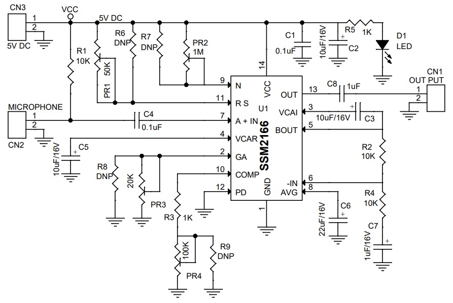
Schematic
Parts List
| NO | QNTY | REF | DESC | MANUFACTURER | SUPPLIER | PART NO |
|---|---|---|---|---|---|---|
| 1 | 1 | CN1, CN2, CN3 | 2 PIN MALE HEADER PITCH 2.54MM | WURTH | DIGIKEY | 732-5315-ND |
| 2 | 2 | C1,C4 | 0.1uF/50V | MURATA/YAGEO | DIGIKEY | |
| 3 | 3 | C2,C3,C5 | 10uF/16V | MURATA/YAGEO | DIGIKEY | |
| 4 | 1 | C6 | 22uF/16V | MURATA/YAGEO | DIGIKEY | |
| 5 | 1 | C7 | 1uF/16V | MURATA/YAGEO | DIGIKEY | |
| 6 | 1 | C8 | 1uF/16V | MURATA/YAGEO | DIGIKEY | |
| 7 | 1 | D1 | LED SMD SIZE 0805 | OSRAM | DIGIKEY | 475-1278-1-ND |
| 8 | 1 | PR4 | 100K TRIMMER POT | BOURNS | DIGIKEY | 3362P-104LF-ND |
| 9 | 1 | PR2 | 1M TRIMMER POT | BOURNS | DIGIKEY | 3362P-105LF-ND |
| 10 | 1 | PR3 | 20K TRIMMER POT | BOURNS | DIGIKEY | 3362P-203LF-ND |
| 11 | 3 | R1,R2,R4 | 10K | MURATA/YAGEO | DIGIKEY | |
| 12 | 2 | R3,R5 | 1K | MURATA/YAGEO | DIGIKEY | |
| 13 | 4 | R6,R7,R8,R9 | DNP | |||
| 14 | 1 | U1 | SSM2166 | ANALOG | DIGIKEY | 2156-SSM2166S-AD-ND |
| 15 | 1 | PR1 | 50K TRIMMER POT | BOURNS | DIGIKEY | 3362P-503LF-ND |
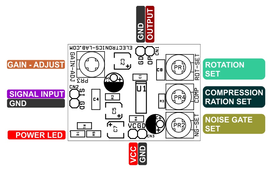
Connections
Gerber View
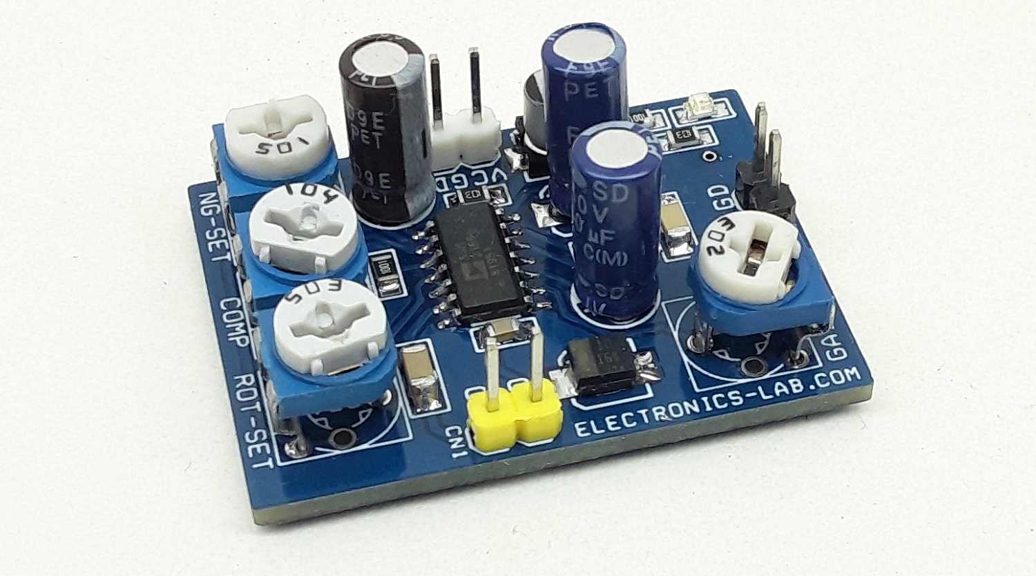
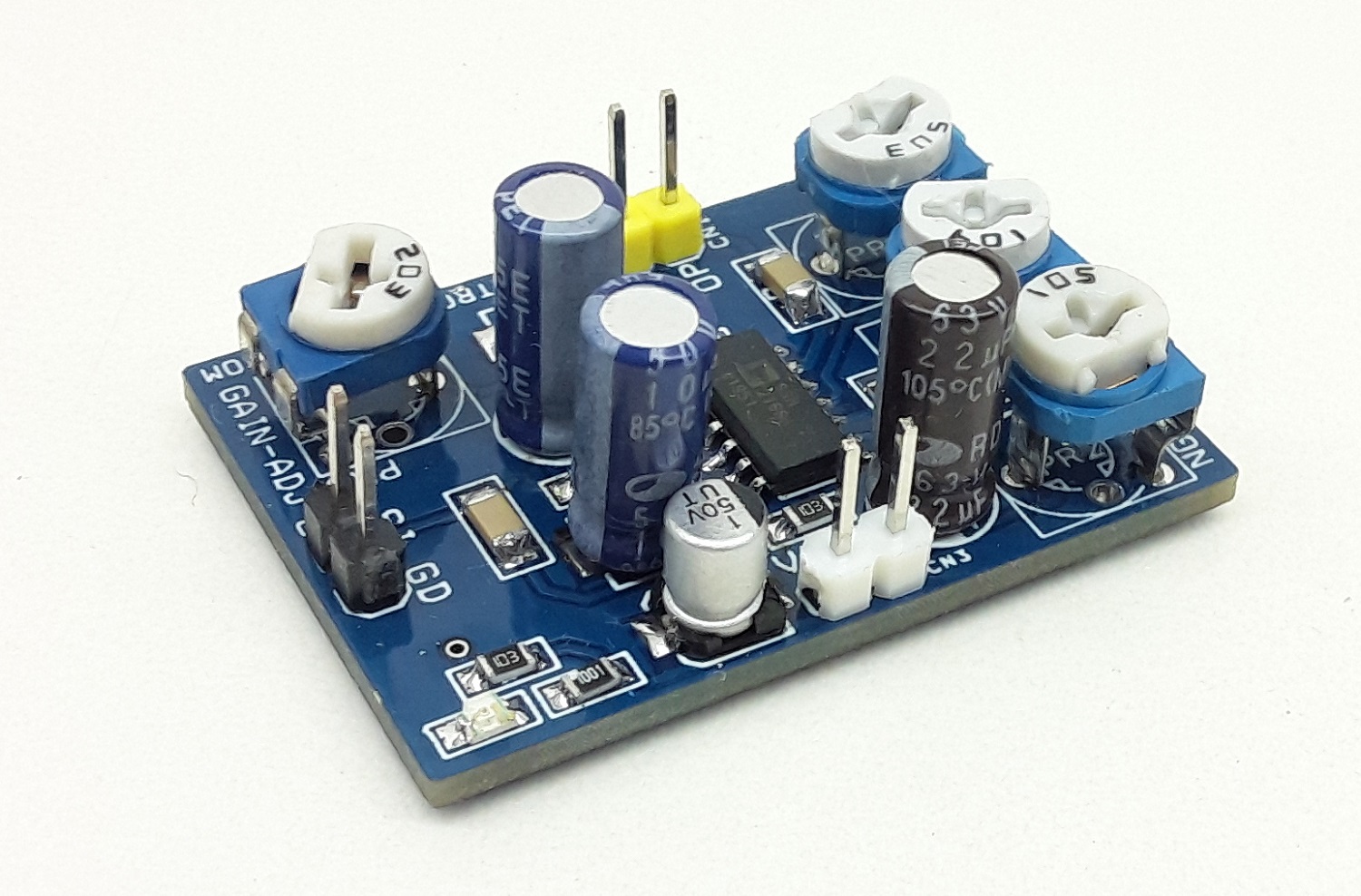
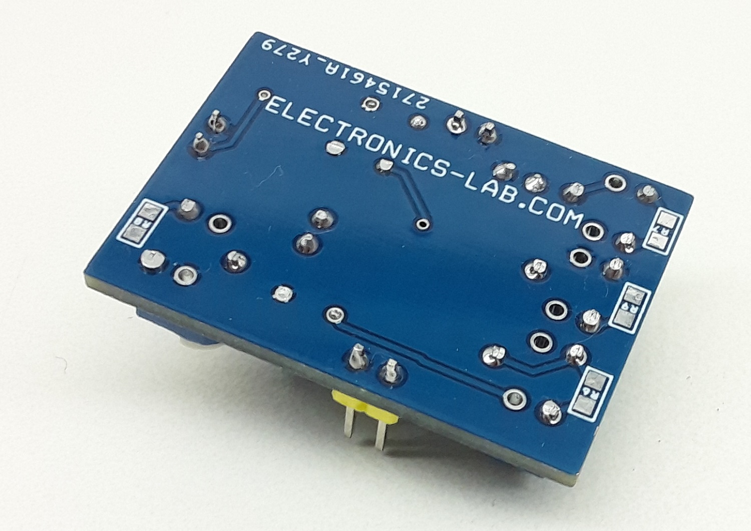
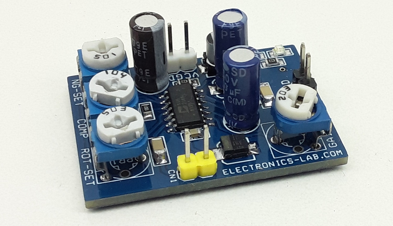
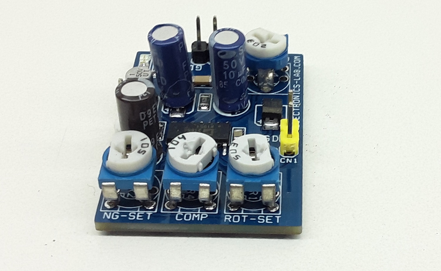
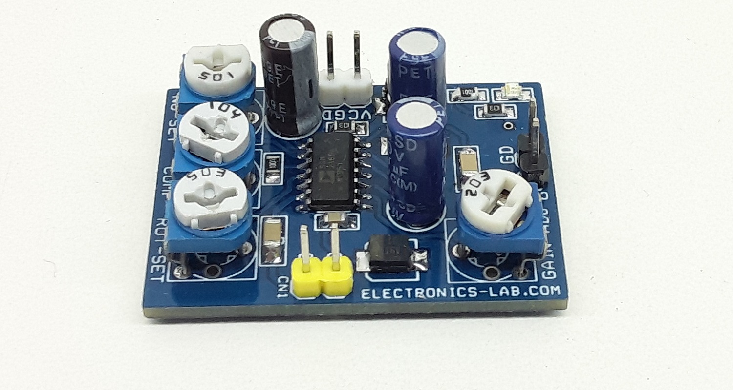
Photos
can phantom power be added from the ssm2019 circuit by cutting the R1 path and removing c4 ?
How can I get an assembled unit or a PCB for this project…??