E-Lab Interview: Wafer.Space Founder Aims to Make Custom Silicon Accessible Again
Tim Ansell discusses his new low-cost silicon manufacturing service, which is being launched today and offers 1,000 custom ICs for $7k USD.
Wafer.space aims to revolutionize custom silicon manufacturing, bringing the accessibility of PCB prototyping to the world of integrated circuits. Tim ‘mithro’ Ansell previously led Google’s open silicon ecosystem initiatives and has now established wafer.space. His vision is to offer a cost-effective pathway for individuals and small teams to produce real products with custom silicon, providing 1,000 dies for just $7,000 USD.
Tim Ansell discussed his new venture, wafer.space, with Electronics-Lab.
The first crowdfunding campaign for Wafer.Space’s initial fabrication run opens today, Thursday, October 2nd, 2025, and Electronics-Lab wanted to learn more about this endeavor from Tim. The interview notes have been lightly edited for clarity.
The Vision Behind Wafer.Space
Electronics-Lab: You have described wafer.space as “OSH Park but for custom silicon.” This is an analogy for accessible PCB prototyping. Could you elaborate on this vision? How is it different from Efabless?
Tim: I am the person who was behind the Google efforts to push forward the open silicon ecosystem, including the release of the open source PDKs, free shuttle progra,m and collaboration with Efabless. I left Google at the beginning of 2024 to take a well-earned break (after being there for 16 years).
Then at the start of 2025 Efabless collapsed (due to investor disagreements rather than product issues), and the open silicon community lost it’s primary pathway to manufacturing. I had long been frustrated that Efabless had never created a chipIgnite program for GF180MCU, primarily because the technology is significantly cheaper than the SKY130 process. Still, due to working closely with Efabless it didn’t feel right to start a competitor. Now with Efabless gone I decided to step up and created wafer.space.
My primary goal with wafer.space is to focus on providing a low-cost option that enables you to build real products. For this reason we don’t offer support or hand holding. Most shuttle programs only provide at most hundreds of parts, this means you can’t really deliver a product to end users. wafer.space returning 1,000 parts means you can use 100 parts in your first prototype run, which doesn’t work, 100 parts in your second prototype, and then still have more than 500 parts for the first production run that you deliver to your early adopter customers.
Excitingly, Tiny Tapeout has also recently received funding to port their technology to GF180MCU and will be using wafer.space for some future shuttles. This means that you can get started for under $200 USD (or maybe even cheaper once the GF runs are going). You can then upgrade from a small design on Tiny Tapeout to a full custom solution chip with wafer.space
Why 180 nm?
Electronics-Lab: Your first run is on GlobalFoundries’ 180nm process (GF180MCU). What were the key factors in selecting this specific node?
Tim: There are currently three primary open source manufacturable PDKs available, two released during my time at Google (SKY130 & GF180MCU) and once released directly by the foundry (iHP SG13G2).
Both SKY130 and iHP SG13G2 are very comprehensive technologies with lot of unique functionality (SONOS, ReRAM, SiGe devices, etc) produced by small boutique foundries in high cost regions of the world, this drives the cost of production higher.
GF180MCU is a non-frills and cost optimized process technology produced by one of the world’s biggest silicon foundries (GlobalFoundries) in Singapore. This is what allows us to offer the current price profitably with room to reduce costs even further if demand grows.
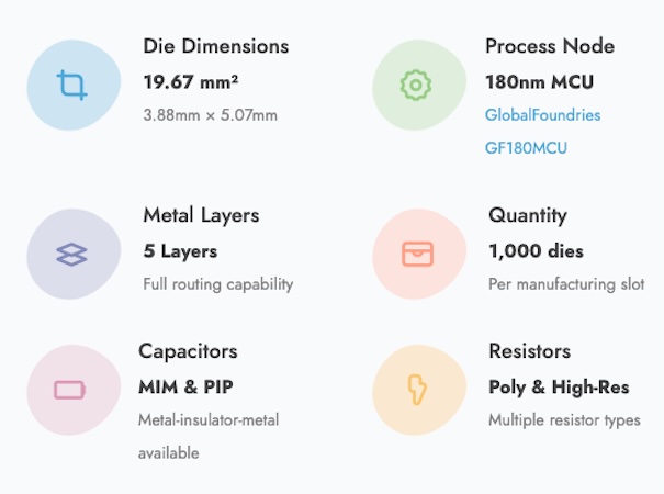
Process details for the Global Foundries 180 nm process used by wafer.space.
I see GF180MCU as the perfect “my first process technology” that is cheap and simple enough to allow anyone to try creating their first custom silicon and use that to create real low volume product.
The Design Flow and Toolchain
Electronics-Lab: The prohibitively expensive EDA toolchain is one of the biggest historical barriers to ASIC design. What does the design and verification flow look like for a wafer.space customer?
Tim: Wafer.space doesn’t provide any tooling support. People are welcome to use whatever tools for design that they wish (proprietary or open source).
The open silicon community (such as the FOSSi Foundation and the IEEE SSCS Chipathon) have built a number of no-cost open source solutions such as LibreLane (a replacement for OpenLane) for digital and Magic, KLayout, xschem and spice for analog. These tools have been battle tested on multiple different process technologies and used for 1,000s of tape outs through both free programs like Google’s OpenMPW program and iHP’s sponsor or paid runs like Efabless’ chipIgnite or foundries typical MPW programs. There is still a lot more work to make things easier, smoother and better integrated — but that is the case for everything!
Wafer.space only checks if the provided files are manufacturable. The customer is responsible for any other verification they wish to do. Wafer.space will provide a fully automated flow where customers provide their GDS f,iles and DRC checking is performed with errors automatically reported. This automation allows customers to quickly get feedback at any time of the day without having to wait for humans to be available, this reduces costs to wafer.space which we pass onto the end customers. These checking tools will also be available for users to run locally and get the same information.
From GDSII to Packaged ICs
Electronics-Lab: The offer of 1,000 ICs for $7,000 is very specific. Could you break down what an engineer receives for that price?
Tim: $7k USD gets your 1,000 bare die. For the early runs we are also offering an option for $8.5k USD to get packaging included via chip-on-board wire bonding (using provided padring and PCB templates) compatible with popular form factors.
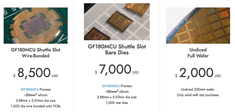
The ASIC deliverable options from wafer.space.
Longer term, wafer.space is working with a number of low cost PCBA partners (like PCB Way, JLC PCB, Seeed, and others) who will offer mounting and wire bonding wafer.space die onto PCBs as part of their PCBA service (PCBA services who are interested in providing services to wafer.space’s customers should email partner@wafer.space).
Wafer.space is also offering the option to purchase full undiced wafers. A number of customers from sensors, MEMS, and nanofluidics research areas have indicated their intent to buy these and build more structures on top of the wafer for unique solutions.
GF wafers are tested for defects and compliance with specification during manufacturing. As a battle-tested process technology in production for almost 30 years, yields are extremely high. Wafer.space is also looking into our own verification structures to make sure that GF is meeting their specification too (and eventually to allow future optimizations).
The Path to Production
Electronics-Lab: This initial crowdfunded run is an exciting start, but engineers considering this for a commercial product will be thinking about the future. What is the long-term vision for wafer.space?
Tim: The frequency of wafer.space runs will be driven by the demand. Our current expectation is that quarterly runs will happen in 2026. I would like to reach a month run schedule.
Two stats that I like to dream about;
- FIRST Robotics, which has helped turn many high schoolers into roboticists had over 3,000 teams in their 2025 season and it costs ~$10k USD to be involved. If we got 15% as many groups (450 submissions) then I would need to do one run a month since each runs has 40 slots.
- There are ~30,000 high schools in the US, if 50% of high schools submitted just one project a year, then I would need to do roughly one run every day. This could even be a small after school club, not even part of the school curriculum.
Another thing to note is that GlobalFoundries offers a wide range of different process technologies. If wafer.space is successful, it is likely we will explore expanding to other technologies in partnership with GF. We may also explore expanding to other foundries. However, for now our primary focus is on making sure our first few runs are successful.
Electronics-Lab: And, if a project prototyped on this run is successful, is there a clear and supported path for a customer to move from their initial 1,000 units to a higher-volume production run of 10,000 or 100,000+ units?
Tim: I think it is worth noting that there are a huge number of market spaces that could benefit from their own customized silicon but don’t need significant number of parts. Previously, silicon manufacturing cost meant that only market spaces that needed >100,000+ units were able to get custom silicon.
If a customer has never created a silicon design before, then Tiny Tapeout will soon be the cheapest way (under $200 USD) to do your first design with GF180MCU technology, getting you back 1-2 parts. If a customer needs more than 1,000 units, they can purchase multiple slots, and repeat orders of the same design are certainly welcome. It is better to think of wafer.space as low volume manufacturing which just happens to be also useful for some people’s prototyping.
Customer should be able to move from wafer.space to manufacturing directly with GlobalFoundries or one of their partners without modifying their design.
Featured image background used courtesy of Adobe Stock. All other images used courtesy of wafer.space.


