
Efinix Extends Sapphire SoC Family With 64-Bit RISC-V Core
The new Sapphire RV64 brings larger memory spaces, deeper caches, and Linux-ready features to FPGA-based embedded designs, scaling up from Efinix's 32-bit cores.
Efinix has announced the Sapphire RV64, a 64-bit RISC-V processor core that joins the company’s existing 32-bit Sapphire SoC suite. Aimed at embedded designs that have outgrown the memory, cache, and I/O ceilings of 32-bit cores, yet still call for the low power and flexibility of an FPGA, the new core is built on the RISC-V Instruction Set Architecture (ISA) and can be tailored to the task at hand.
Stepping Up From 32 Bits
Efinix pitches the RV64 as the natural next rung for customers already working with its Sapphire RV32 cores, who can scale up without re-architecting their systems. The design is similar to the open-source VexiiRiscv, tuned here for Efinix FPGA fabrics, and it runs a seven-stage pipeline implementing the RISC-V64IM ISA. Optional extensions (A, F, D, C, Zba, Zbb, Zbs, and Zicbom) widen the instruction set, and up to four processors can share a single SoC. Carried over from the RV32 architecture is the custom instruction interface, which offers 1,024 identifiers and lets designers push hot spots into FPGA logic through a software-defined flow.
Memory, Caches, and Debug
Memory headroom is where the jump to 64 bits earns its keep. On-chip RAM spans 4 to 512 KB and sits behind multi-way L1 instruction and data caches, with an optional L2 cache of 64 to 512 KB beyond them. A branch predictor and both hardware and software pre-fetchers can be switched on, and an optional SV39 memory management unit prepares the core for Linux. Off-chip, the built-in controller talks to DDR3, HyperRAM, and LPDDR4x devices; LPDDR4x operation reaches 3,200 Mbps, and supported module sizes run from 4 MB up to 8 GB.
Debugging follows the standard RISC-V debug specification and offers up to four hardware breakpoints and four performance counters. It also supports co-debug with the FPGA debugger natively.
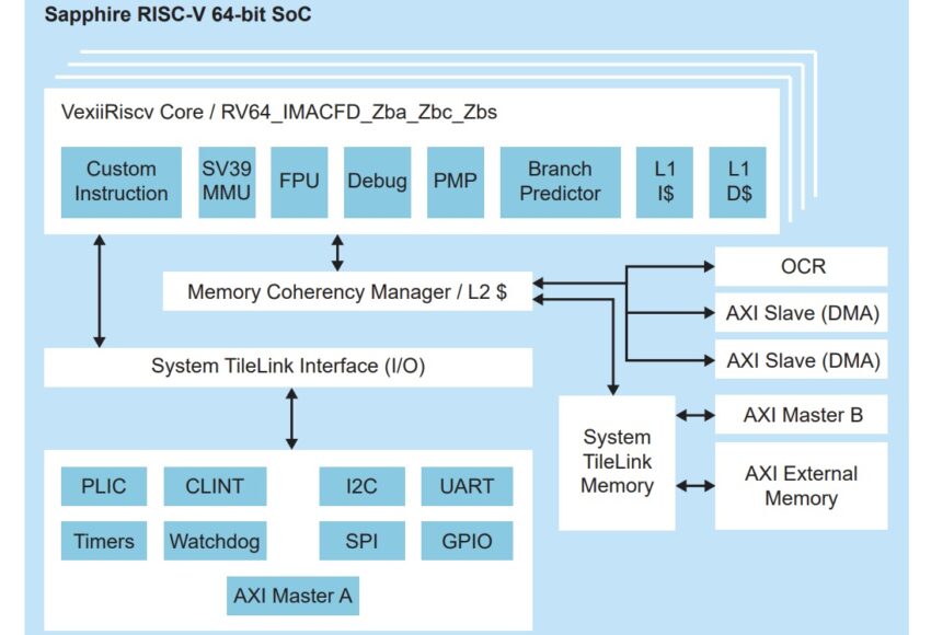
Up to four VexiiRiscv cores share the coherency manager, L2 cache, and I/O fabric of the Sapphire RV64 SoC. Image used courtesy of Efinix
Configuration and Device Support
Efinity IP Manager configures every Sapphire core, 32-bit or 64-bit. The Efinity Integrated Development Environment handles the RTL-to-bitstream flow, while an Eclipse-based software environment covers development, debugging, and BSP integration. The system clock is adjustable from 20 to 400 MHz, although the fMAX of a given design sets the real limit.
The IP page’s utilization tables show how configuration and device choice interact. On a Titanium Ti375, a basic single-core build with L2 cache consumes 14,258 logic and adder resources and reaches 278 MHz; an advanced build, with nearly every extension enabled, uses 27,250 and reaches 252 MHz. The same two builds on a Trion T120 top out at 77 and 65 MHz, respectively. Sapphire RV64 is available for all Titanium and Topaz FPGAs and for Trion devices from the T20 upward, though some features, such as the DDR controller, depend on hardened blocks that only certain devices include.
All told, the Sapphire RV64 hands FPGA-based designs a roomier, more Linux-friendly processor without abandoning the configurability that defines the Sapphire family. Embedded Linux platforms, machine vision, industrial automation, and edge AI systems, anywhere big memory spaces meet a craving for a little custom hardware acceleration, look like natural homes for it. If you’ve bumped your head against the ceiling of a 32-bit soft core, this one is worth a close look.


