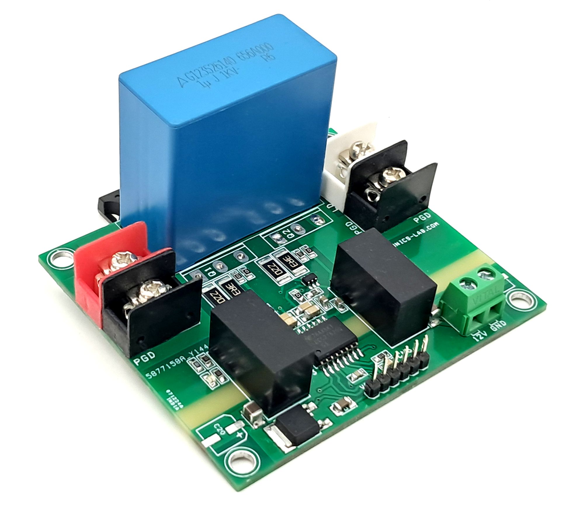
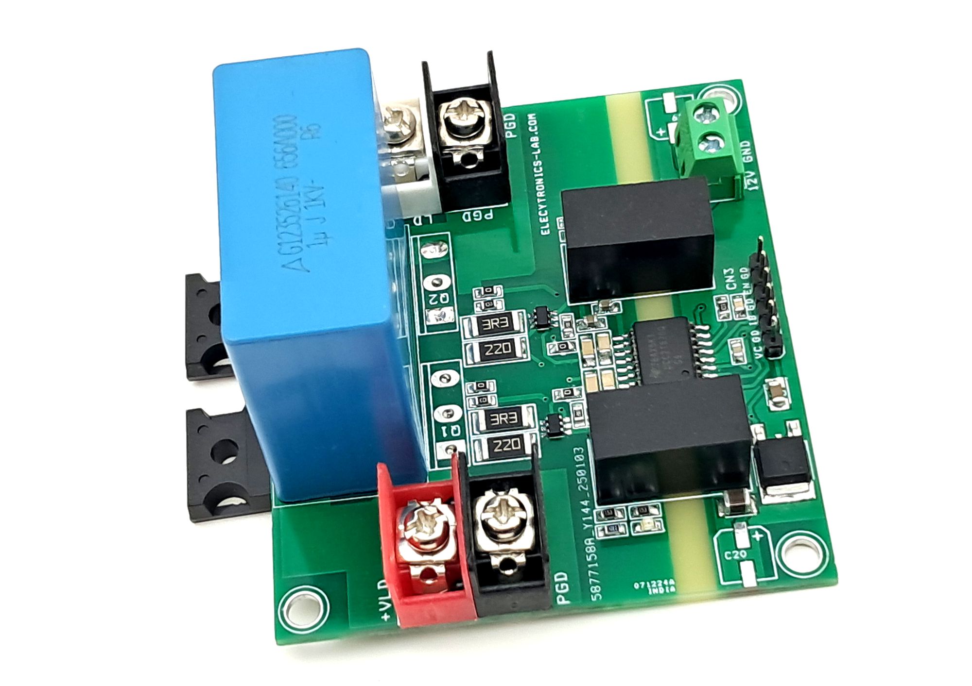
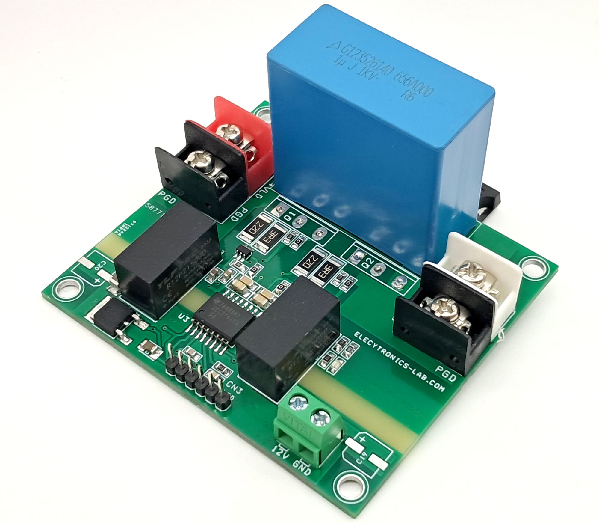
High-Voltage Isolated Half-Bridge Driver (Up to 1kV)
A fully isolated 1kV half-bridge driver for high-voltage use. Features isolated DC-DC converters, 1.2KV IGBTs, power LEDs, and 2.5kV galvanic isolation between signal and power grounds. Accepts 12V DC input and PWM control.
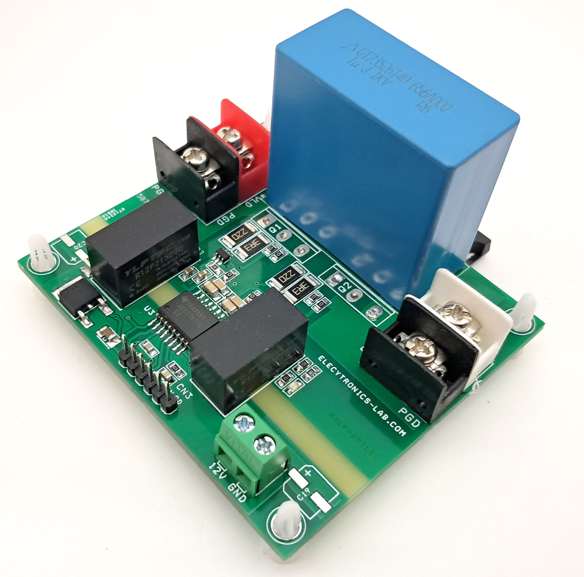
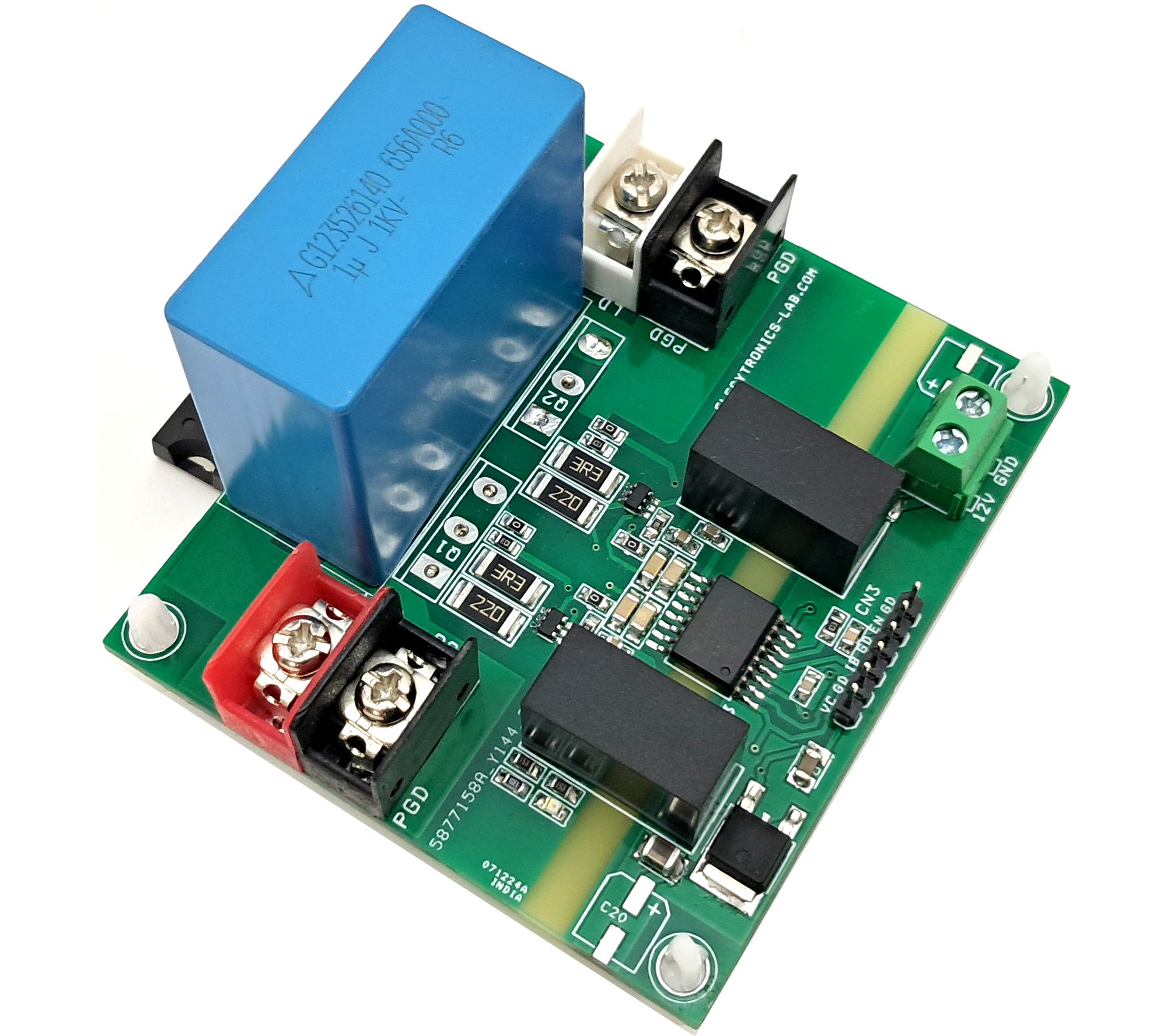
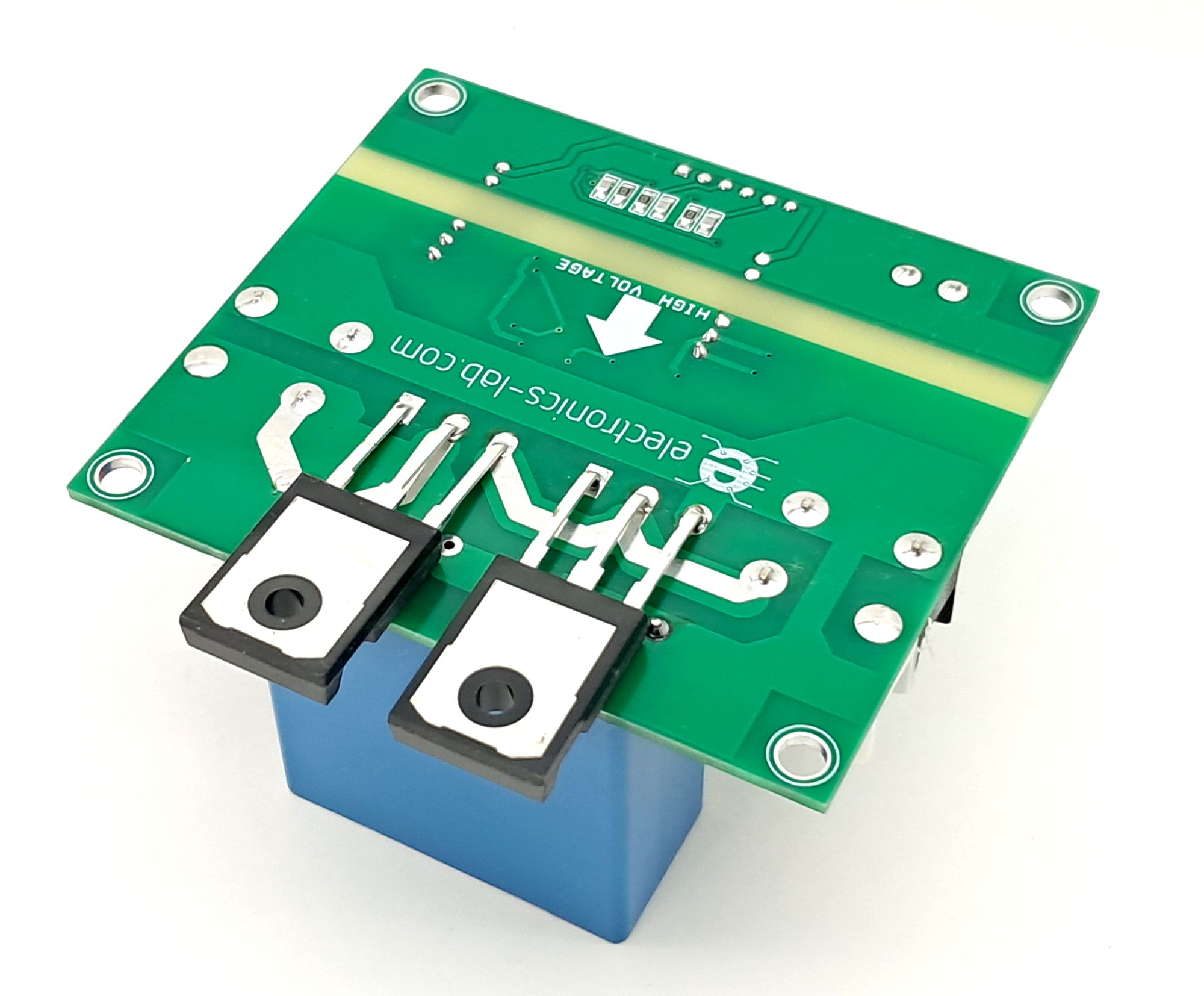
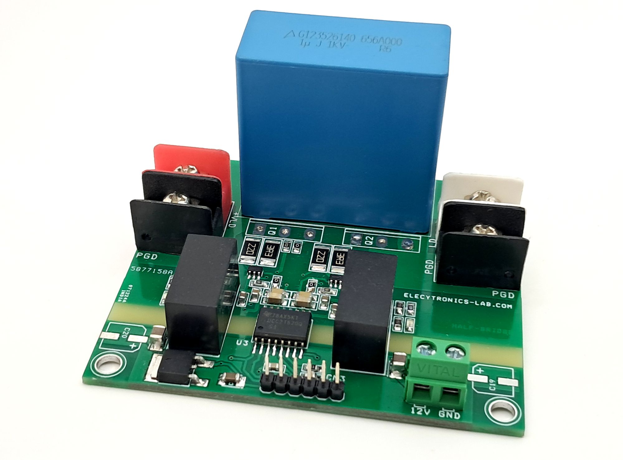
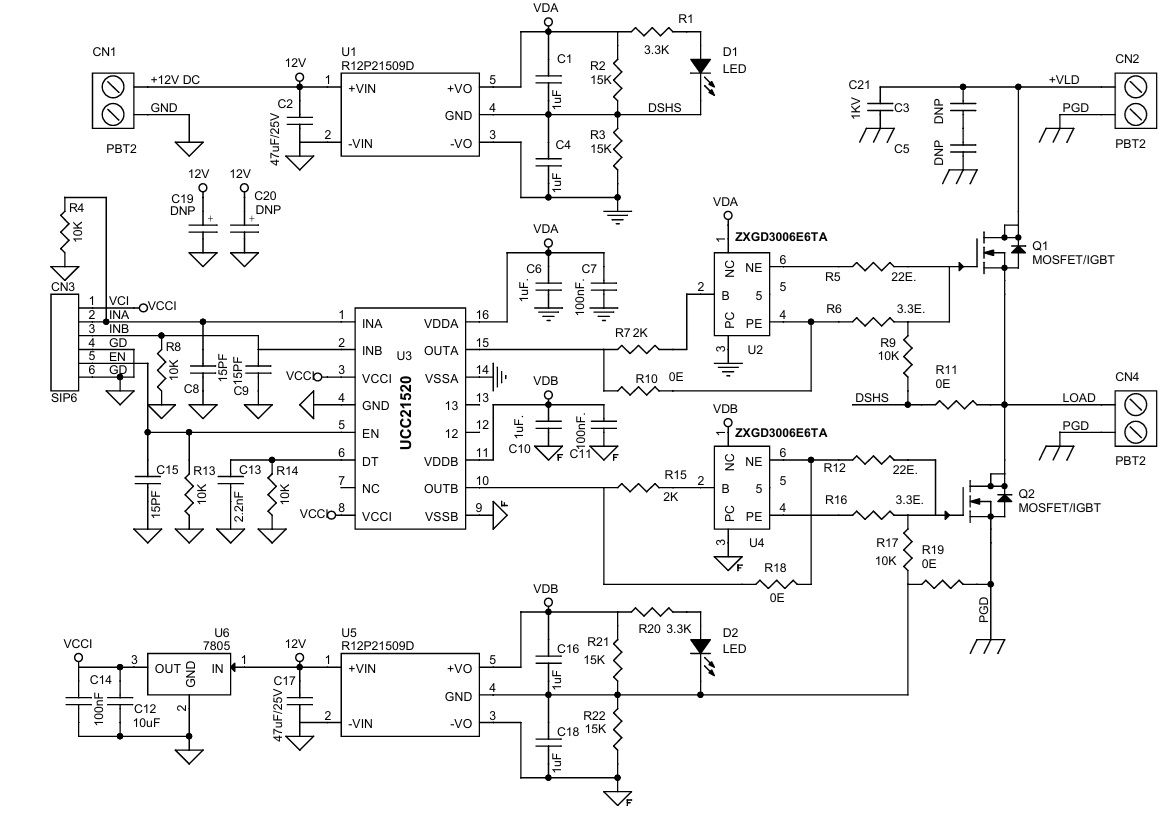
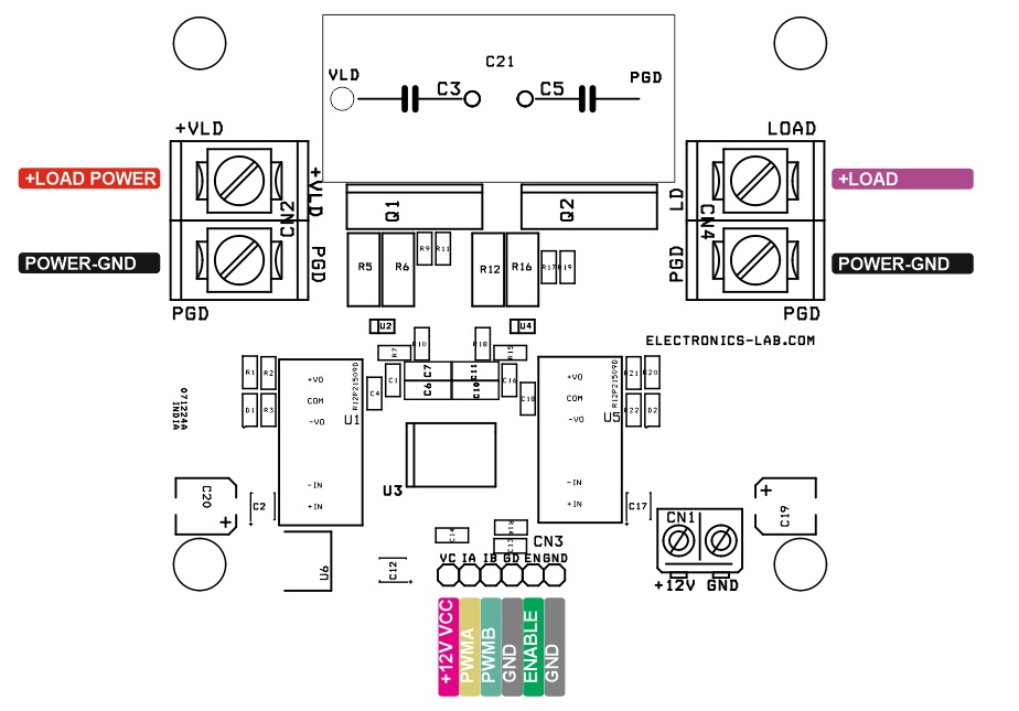
This fully isolated half-bridge driver is designed for high-voltage applications up to 1kV. It features 2 x 2W isolated DC-DC converters to independently power the low-side and high-side switching elements. The board is assembled with 1.2KV IGBTs, Two power LEDs provide visual indication of power presence for both the low-side and high-side gate drivers. The signal ground is galvanically isolated from the power ground, allowing it to be connected to any potential up to 2.5kV. Barrier connectors are provided for the load and its power supply. A screw terminal connector facilitates the 12V DC input for the gate driver circuitry. A LM78M05 regulator provides a 5V supply to the logic side of the gate driver input circuit. A header connector allows for PWM input via channels A and B, as well as enable/disable control.
The driver incorporates the following key components:
- UCC21520 Isolated Half-Bridge Driver Chip
- Two Isolated DC-DC Converters (one for each side), R12P21509D
- ZXGD30006 High-Current Gate Driver Chip
- Two 1.2KV/40Amp, FGH40T120SMD-ND
Important Considerations:
- Select appropriate IGBTs based on your specific power and frequency requirements.
- This board is suitable for DC bus voltages up to 800V Max 1KV.
- Testing was performed using a 6.5kHz TTL signal and a 105V DC power supply.
Features
- Power Supply Gate Driver 12V DC
- Power Supply Load 800V DC (Max 1KV)
- Gate Drive DC-DC Converter Voltage Output +15V / -9V
- On Board 5V Regulator to power the Gate Driver Input side circuit
- Common-Mode Transient Immunity (CMTI) greater than 125V/ns
- High Gate-drive Currents (up to 10A source and sink)
- Surge immunity up to 10kV
- Programmable overlap and dead time
- Fast disable for power sequencing
- 8000VPK reinforced Isolation per DIN EN IEC 60747-17 (VDE 0884-17)
- 7kVRMS isolation for 1 minute per UL 1577 (UCC21520)
- 4 x 4MM PCB Mounting Holes
- PCB Dimensions 79.69 x 70.17 mm
Driving MOSFETS/SIC MOSFETS
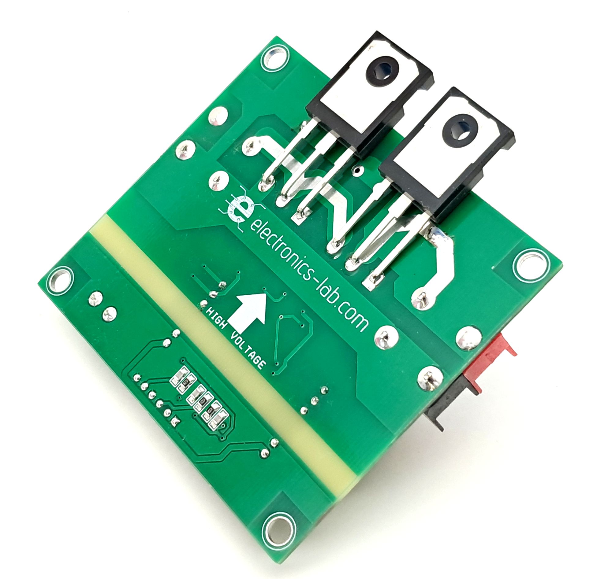
The board is configured and tested with IGBTs, however this board can also use with MOSFETs and SiC MOSFETs. When using MOSFETs or SiC MOSFETs, it is crucial to select appropriate gate driver resistors based on the device’s capacitance and source/sink current requirements. The following RECOM DC-DC converters are available to drive various power devices, including MOSFETs, IGBTs, and SiC MOSFETs. Q1 and Q2 are designed for TO-247 packages, but TO-220 packages can also be installed.
- R12P22005D* 2 +20/-5 SiC MOSFETs
- R12P21503D* 2 +15/-3 SiC MOSFETs
- R12P21509D* 2 +15/-9 IGBTs
- R12P1509D 1 +15/-9 IGBTs
- R12P06S* 1 +6 GaN
- R12P12S 1 +12 Cascode/Si MOSFET
Applications
- Switch Mode Power Supply (LLC half-bridge)
- Asymmetric duty cycle half-bridge (forward and flyback)
- Active clamp half-bridge (forward and flyback)
- Full-bridge / phase-shifted full-bridge
- Synchronous boost converter
- Synchronous buck converter
- 3Phase Inverters
Disable Pin
Setting the DISABLE pin high shuts down both outputs simultaneously. Grounding (or left open) the DISABLE pin allows the UCC21520 and the UCC21520A to operate normally. The DISABLE response time is in the range of 20 ns and quite responsive, which is as fast as propagation delay. The DISABLE pin is only functional (and necessary) when VCCI stays above the UVLO threshold. It is recommended to tie this pin to ground if the
DISABLE pin is not used to achieve better noise immunity, and it is recommended to bypass using a ≈1-nF low ESR/ESL capacitor close to DIS pin when connecting DIS pin to a micro controller with distance.
Programmable Dead-Time (DT) Pin
DT Pin Connected to a Programming Resistor R14 Between DT and GND Pins
The appropriate RDT value can be determined from Equation, where RDT is in kΩ and tDT is in ns:
- tDT=10XRDT(R14)
The steady state voltage at DT pin is around 0.8 V, and the DT pin current will be less than 10uA when RDT=100kΩ. When using RDT> 5kΩ, parallel capacitor C13 is used better noise immunity and better dead time matching between two channels.
Here is a suggestion on how to select an appropriate dead time for UCC21520:
- DT-Setting=DTREQ + TFSYS + TRSYS – TD(ON)
where
- DTsetting: UCC21520 dead time setting in ns, DTSetting = 10 × RDT-R14 (in kΩ).
- DTReq: System required dead time between the real VGS signal of the top and bottom switch with enough margin, or ZVS requirement.
- TF_Sys: In-system gate turn-off falling time at worst case of load, voltage/current conditions.
- TR_Sys: In-system gate turn-on rising time at worst case of load, voltage/current conditions.
- TD(on): Turn-on delay time, from 10% of the transistor gate signal to power transistor gate threshold.
In the example, DTSetting is set to 100 ns.
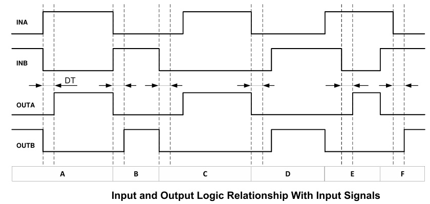
Inputs and Outputs
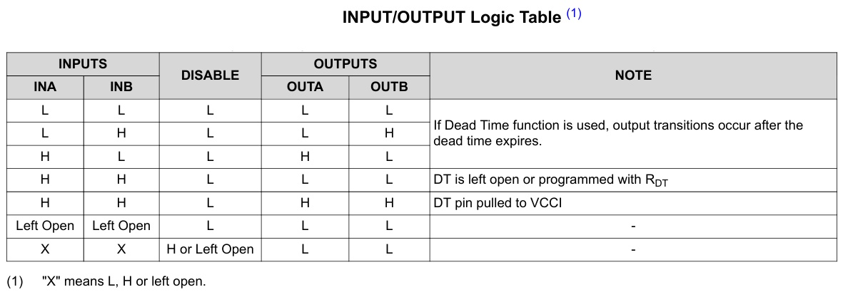
- Condition A: INB goes low, INA goes high. INB sets OUTB low immediately and assigns the programmed dead time to OUTA. OUTA is allowed to go high after the programmed dead time.
- Condition B: INB goes high, INA goes low. Now INA sets OUTA low immediately and assigns the programmed dead time to OUTB. OUTB is allowed to go high after the programmed dead time.
- Condition C: INB goes low, INA is still low. INB sets OUTB low immediately and assigns the programmed dead time for OUTA. In this case, the input signal’s own dead time is longer than the programmed dead time. Thus, when INA goes high, it immediately sets OUTA high.
- Condition D: INA goes low, INB is still low. INA sets OUTA low immediately and assigns the programmed dead time to OUTB. INB’s own dead time is longer than the programmed dead time. Thus, when INB goes high, it immediately sets OUTB high.
- Condition E: INA goes high, while INB and OUTB are still high. To avoid overshoot, INA immediately pulls OUTB low and keeps OUTA low. After some time OUTB goes low and assigns the programmed dead time to OUTA. OUTB is already low. After the programmed dead time, OUTA is allowed to go high.
- Condition F: INB goes high, while INA and OUTA are still high. To avoid overshoot, INB immediately pulls OUTA low and keeps OUTB low. After some time OUTA goes low and assigns the programmed dead time to OUTB. OUTA is already low. After the programmed dead time, OUTB is allowed to go high.
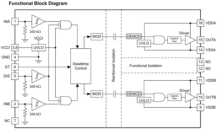
The UCC21520 is an isolated dual-channel gate driver with 4A source and 6A sink peak current. It is designed to drive power MOSFETs, IGBTs, and SiC MOSFETs up to 5MHz.The input side is isolated from the two output drivers by a 5.7kVRMS reinforced isolation barrier, with a minimum of 125V/ns common-mode transient immunity (CMTI). Internal functional isolation between the two secondary-side drivers allows a working voltage of up to 1500VDC.Every driver can be configured as two low-side drivers, two high-side drivers, or a half-bridge driver with programmable dead time (DT). A disable pin shuts down both outputs simultaneously when it is set high, and allows normal operation when left open or grounded. As a fail-safe measure, primary-side logic failures force both outputs low. Each device accepts VDD supply voltages up to 25V. A wide input VCCI range from 3V to 18V makes the driver suitable for interfacing with both analog and digital controllers. All supply voltage pins have under voltage lock-out (UVLO) protection. With all these advanced features, the UCC21520 enables high efficiency, high power density, and robustness. Each device accepts VDD supply voltages up to 25 V. A wide input VCCI range from 3 V to 18 V makes the driver suitable for interfacing with both analog and digital controllers. All supply voltage pins have under voltage lock-out (UVLO) protection. With all these advanced features, the UCC21520 and the UCC21520A enable high efficiency, high power density, and robustness in a wide variety of power applications.
Schematic
Parts List
| NO. | QNTY. | REF. | DESC | MANUFACTURER | SUPPLIER | SUPPLIER PART NO |
|---|---|---|---|---|---|---|
| 1 | 2 | CN2,CN4 | 2 PIN BARRIER BLOCK PITCH 9.53MM | TE CONNECTIVITY | DIGIKEY | A98481-ND |
| 2 | 1 | CN3 | 6 PIN MALE HEADER PITCH 2.54MM | WURTH | DIGIKEY | 732-5319-ND |
| 3 | 4 | C1,C4,C16,C18 | 1uF/50V CERAMIC SMD SIZE 0805 | YAGEO/MURATA | DIGIKEY | |
| 4 | 2 | C2,C17 | 47uF/25V CERAMIC SMD SIZE 1210 | YAGEO/MURATA | DIGIKEY | |
| 5 | 4 | C3,C5,C19,C20 | DNP | |||
| 6 | 2 | C6,C10 | 1uF/50V CERAMIC SMD SIZE 1206 | YAGEO/MURATA | DIGIKEY | |
| 7 | 2 | C7,C11 | 100nF/50V CERAMIC SMD SIZE 1206 | YAGEO/MURATA | DIGIKEY | |
| 8 | 3 | C8,C9,C15 | 15PF/50V CERAMIC SMD SIZE 0805 | YAGEO/MURATA | DIGIKEY | |
| 9 | 1 | C12 | 10uF/25V CERAMIC SMD SIZE 0805 | YAGEO/MURATA | DIGIKEY | |
| 10 | 1 | C13 | 2.2nF/50V CERAMIC SMD SIZE 0805 | YAGEO/MURATA | DIGIKEY | |
| 11 | 1 | C14 | 100nF/50V CERAMIC SMD SIZE 0805 | YAGEO/MURATA | DIGIKEY | |
| 12 | 1 | C21 | 1uF/1KV EPCOS 42X20MM | EPCOS | DIGIKEY | 495-B32656A0105J000-ND |
| 13 | 2 | D1,D2 | LED RED SMD SIZE 0805 | OSRAM | DIGIKEY | 475-1278-1-ND |
| 14 | 2 | Q1,Q2 | MOSFET/IGBT/FGH40T120SMD | ONSEMI | DIGIKEY | FGH40T120SMD-ND |
| 15 | 2 | R1,R20 | 3.3K 5% SMD SIZE 0805 | YAGEO/MURATA | DIGIKEY | |
| 16 | 4 | R2,R3,R21,R22 | 15K 5% SMD SIZE 0805 | YAGEO/MURATA | DIGIKEY | |
| 17 | 6 | R4,R8,R9,R13,R14,R17 | 10K 5% SMD SIZE 0805 | YAGEO/MURATA | DIGIKEY | |
| 18 | 2 | R5,R12 | 22E/2W 5% SMD SIZE 2512 | YAGEO/MURATA | DIGIKEY | |
| 19 | 2 | R6,R16 | 3.3E/2W 5% SMD SIZE 2512 | YAGEO/MURATA | DIGIKEY | |
| 20 | 2 | R7,R15 | 2K 1% SMD SIZE 0805 | YAGEO/MURATA | DIGIKEY | |
| 21 | 4 | R10,R11,R18,R19 | 0E SMD SIZE 0805 | YAGEO/MURATA | DIGIKEY | |
| 22 | 2 | U1,U5 | R12P21509D | RECOM POWER | DIGIKEY | 945-2800-ND |
| 23 | 2 | U2,U4 | ZXGD3006E6TA | DIODE INC | DIGIKEY | ZXGD3006E6TADICT-ND |
| 24 | 1 | U3 | UCC21520 | TI | DIGIKEY | 296-48796-1-ND |
| 25 | 1 | U6 | LM78M05 | TI | DIGIKEY | MC78M05CDTGOS-ND |
| 26 | 1 | CN1 | 2 PIN SCREW TERMINAL PITCH 5.08MM | PHOENIX | DIGIKEY | 277-1247-ND |
Connections
UCC21520 Block Diagram
Input/Output Waveforms
Input/Output Logic Table