Isolated Full-Duplex RS-485 Transceivers
This module is an isolated full-duplex differential line driver and receiver for TIA/EIA RS485/RS422 applications. The module is ideal for long transmission lines because the ground loop is broken to allow for a much larger common-mode voltage range.
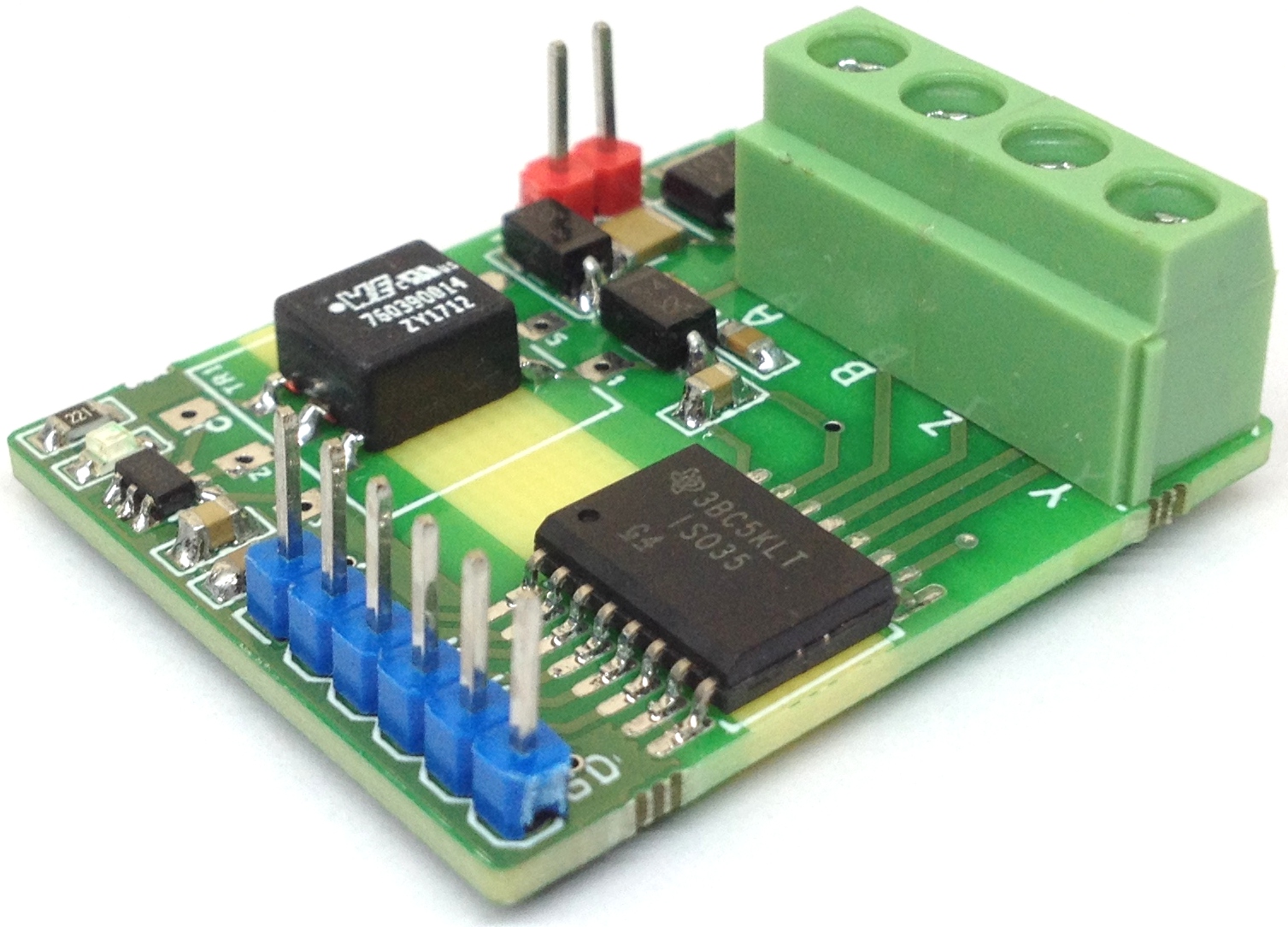
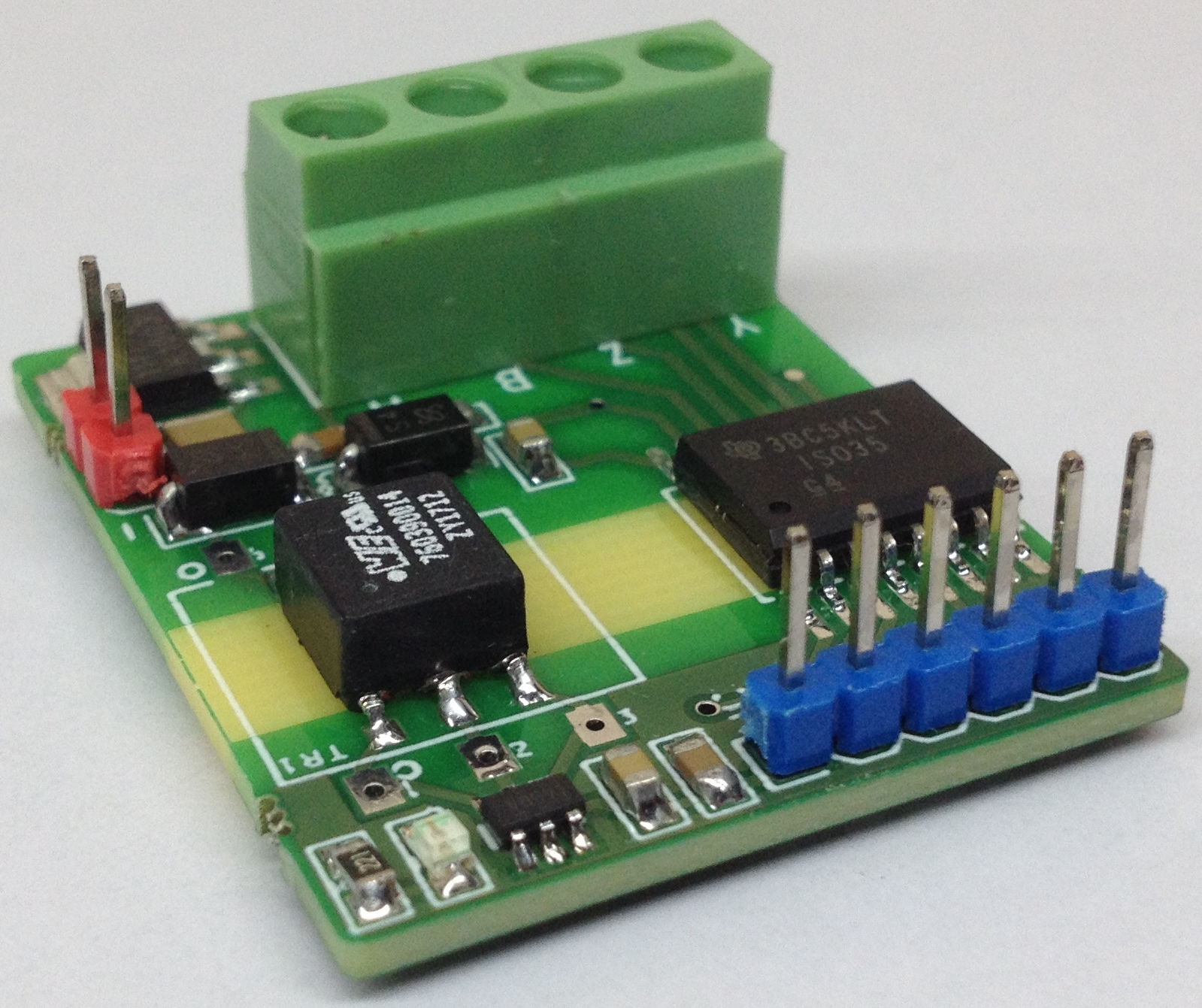
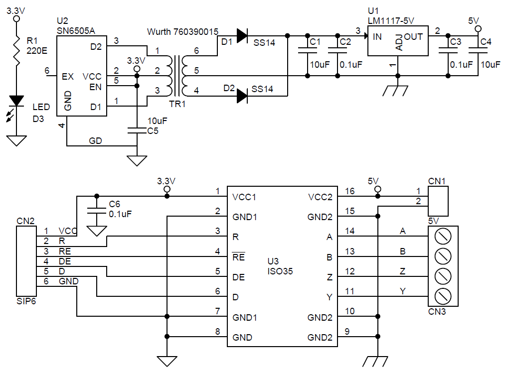
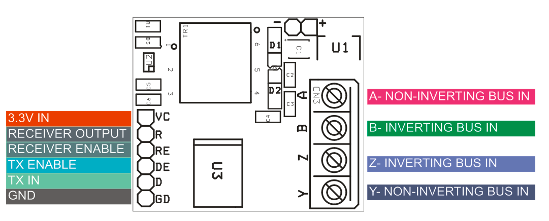
This module is an isolated full-duplex differential line driver and receiver for TIA/EIA RS485/RS422 applications. The module is ideal for long transmission lines because the ground loop is broken to allow for a much larger common-mode voltage range. The symmetrical barrier of the device is tested to provide isolation of 2500Vrms between bus line Trans-receiver and the logic-level interface. The circuit works with a single supply 3.3V input. SN6505 Chip and Wurth Elekronics 760390015 transformer help to generate 5V DC to power up isolated circuitry. Module has been designed using ISO35 IC which is an isolated full-duplex RS485 trans-receiver, SN6505 IC used to form isolated DC-DC converter to power up the bus side of isolated circuitry of ISO35, LM1117-5V IC regulates the output of DC-DC converter and provides 5V DC. CN2 6 Pin header connector provided to power up the board and micro-controller interface, CN3 for Full-Duplex communication. CN1 is for AUX power 5V DC.
Any cables I/O can be subjected to electrical noise transients that can cause damage to the transceiver and/or nearby sensitive circuitry if they are of sufficient magnitude and duration. This module can significantly increase protection and reduce the risk of damage to an expensive control circuit. The device can be used for applications like security systems, chemical production, factory automation, motor control circuit, networked security stations, HVAC and building automation networks.
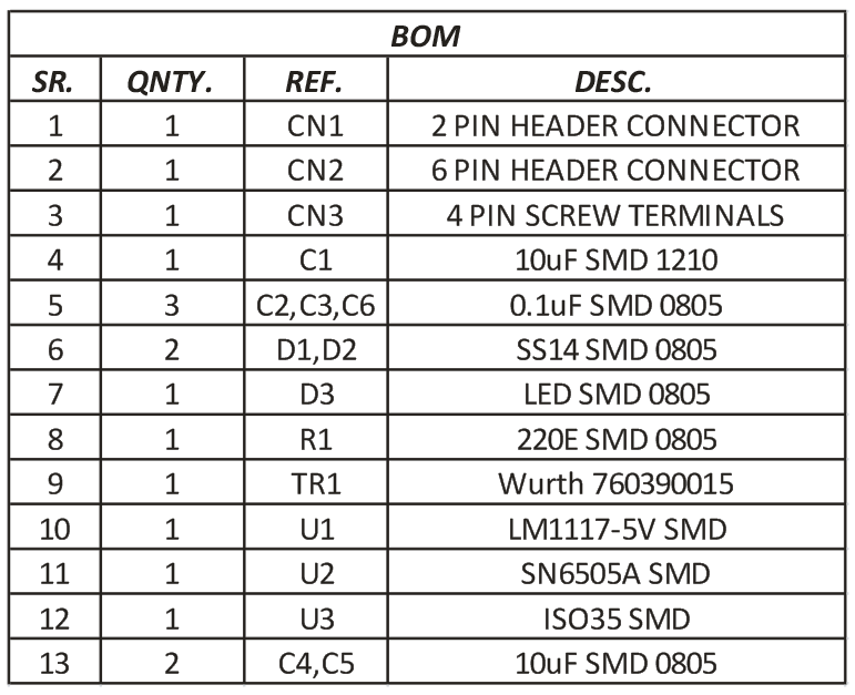
When the driver enable pin, DE, is logic high, the differential outputs Y and Z follow the logic states at data input D. A logic high at D causes Y to turn high and Z to turn low. In this case, the differential output voltage defined as VOD = V(Y) – V (Z) is positive. When D is low, the output states reverse, Z turns high, Y becomes low, and VOD is negative. When DE is low, both outputs turn high-impedance. In this condition the logic state at D is irrelevant. The DE pin has an internal pull-down resistor to ground, thus when left open the driver is disabled (high impedance) by default. The D pin has an internal pull up resistor to VCC, thus, when left open while the driver is enabled, output Y turns high and Z turns low.
When the receiver enable pin, RE, is logic low, the receiver is enabled. When the differential input voltage defined as VID = V(A) – V(B) is positive and higher than the positive input threshold, VIT+, the receiver output, R, turns high. When VID is negative and less than the negative and lower than the negative input threshold, VIT– , the receiver output, R, turns low. If VID is between VIT+ and VIT– the output is indeterminate. When RE is logic high or left open, the receiver output is high-impedance and the magnitude and polarity of VID are irrelevant. Internal biasing of the receiver inputs causes the output to go failsafe-high when the transceiver is disconnected from the bus (open-circuit), the bus lines are shorted (short-circuit), or the bus is not actively driven (idle bus).
Features
- Single Supply 3.3V
- Onboard Isolated DC-DC Converter Provides 5V Output for Bus Side Circuitry
- CN2 Header Connector for Micro-Controller Interface
- 4 Pin Screw Terminal for Full-Duplex Communication
- D3 Power LED
- PCB Dimensions 36.27 x 30.35mm
Schematic
Parts List
Connections
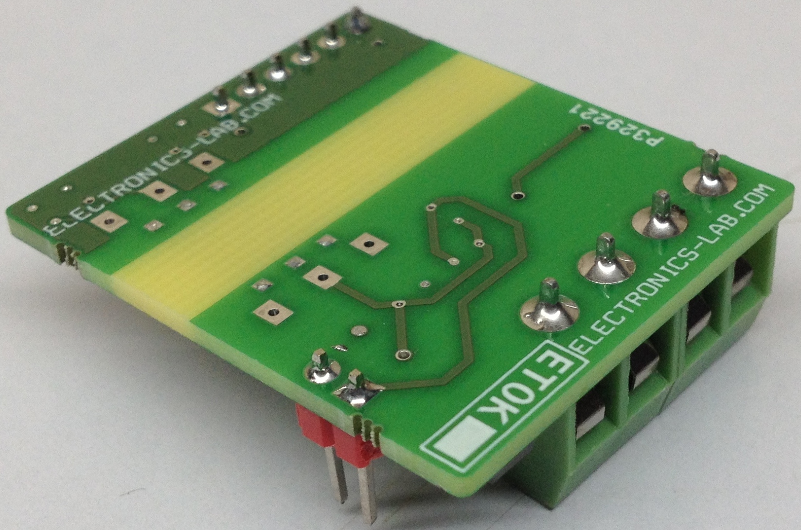
Photos