
Siemens and ASU Launch Online PCB Design Microcredential Program
A new hands-on curriculum trains engineers on industry EDA tools to close the growing hardware design skills gap.
Siemens Digital Industries Software and Arizona State University (ASU) have introduced an online microcredential program in printed circuit board (PCB) design to address what both organizations call a shortage of job-ready board designers. The program, titled “PCB Design Fundamentals: From Discovery to Production,” guides learners through the full board design lifecycle, from initial schematic capture to a production-ready handoff.
The launch coincides with a broader expansion in physical electronics manufacturing, driven by growth in AI infrastructure, electric vehicles, and medical devices. Program materials note that employers increasingly seek candidates fluent in modern Electronic Design Automation (EDA) workflows rather than academic credentials alone. Representatives from both organizations highlighted a widening gap between engineering graduates and the applied, tool-specific skills hiring managers seek, particularly as design teams contend with tighter timelines and fewer experienced engineers to fill open roles.
A Curriculum Built Around Production Workflows
The program totals 40 hours, delivered across four self-paced, ten-hour courses: PCB design basics covering components, materials, and manufacturing; schematic design and circuit development; layout design covering placement, routing, and DRC; and design for manufacturability (DFM) and verification. Coursework is completed using Siemens’ Xpedition software, a PCB design platform used across the aerospace, automotive, and medical device sectors, delivered through a browser-based lab environment. Learners progress through pre-recorded modules in sequence, with each new module unlocking only after the prior one is complete.
No prerequisites are required to enroll, making the program accessible to undergraduate engineering students, technicians, and professionals transitioning from adjacent fields such as mechanical or manufacturing engineering. ASU estimates that a typical learner spends three to four hours per week on the material and completes the program within roughly three months, though the self-paced structure allows for faster or slower progress depending on individual schedules.
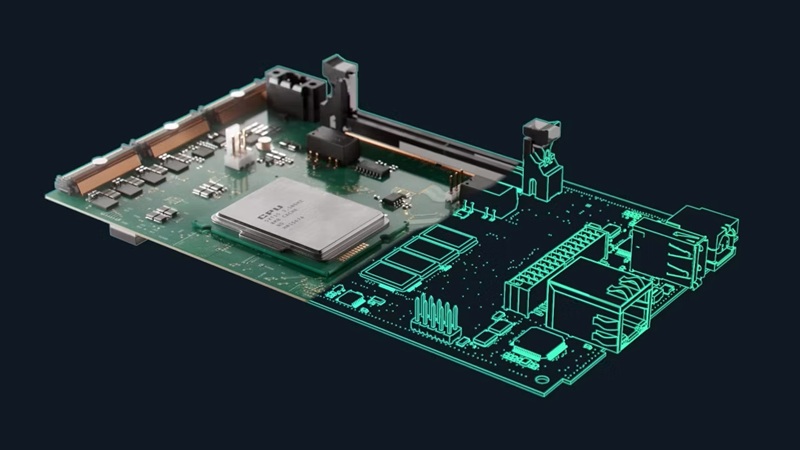
From concept to completed board: the practical, hands-on skillset the program aims to build. Image used courtesy of Siemens
Credentials and Career Placement
Completing all four courses earns learners a Siemens microcredential and a professional certificate from ASU. Both can be displayed on LinkedIn and other professional platforms, giving recruiters a way to verify applied skills beyond a standard degree listing. Graduates are also invited to add their profiles to the Siemens Talent Directory, a database that Siemens and its commercial customers can search when staffing PCB design roles. The program became available on July 28, 2026, with enrollment now open through ASU’s CareerCatalyst platform at an introductory certificate rate of $899.
For engineers eyeing a move into hardware design, or for teams looking to reskill existing staff, the program offers a direct route into modern board design workflows without requiring a return to a full degree program. Its value will likely depend on how widely Xpedition is used at a given employer, since the training is built around that specific toolchain. Even so, the underlying curriculum, spanning schematic capture through DFM and production handoff, closely aligns with the stages of board design that come up in day-to-day engineering work, making it a reasonable option for anyone looking to add PCB layout and verification skills to their resume.
Featured image used courtesy of Adobe Stock


