Lattice Launches Secure Control FPGA Family With Post-Quantum Security
The new MachXO5-NX TDQ FPGA family features full CNSA 2.0-compliant post-quantum cryptography support, hardware Root of Trust, and secure boot functionality.
As quantum computing progresses, the need for cryptographic systems resilient to quantum attacks has become a focus for engineers and security professionals. In response to this evolving threat, Lattice Semiconductor has introduced the MachXO5-NX TDQ FPGA family. This new line of secure control FPGAs features full Commercial National Security Algorithm (CNSA) 2.0-compliant post-quantum cryptography (PQC) support. The MachXO5-NX TDQ FPGAs are based on the Lattice Nexus platform and are designed to provide a comprehensive security solution from boot-up to runtime.

The Lattice MachXO5-NX TDQ devices focus on security, featuring full CNSA 2.0-compliant PQC algorithm support. Image used courtesy of Lattice Semiconductor
The Lattice MachXO5-NX TDQ Family
The Lattice MachXO5-NX TDQ devices integrate a full suite of CNSA 2.0 and NIST-approved PQC algorithms, including ML-KEM for key encapsulation and ML-DSA for digital signatures. For secure code and firmware authentication, the FPGAs also support hash-based LMS and XMSS. The architecture is designed to be “crypto-agile,” providing backward compatibility with classical algorithms such as AES256-GCM, SHA2/3, ECDSA, and RSA. A hybrid cryptographic model allows for the coexistence of classical and PQC algorithms.
A patent-pending architecture also enables in-field cryptographic algorithm updates with anti-rollback protection, allowing for future-proofing of designs. Beyond PQC, the MachXO5-NX TDQ devices incorporate robust hardware security features. This includes a hardware Root of Trust (RoT) with a trusted single-chip boot process and a unique device secret. This hardware-based RoT ensures the integrity of the boot process and the authenticity of the device itself.
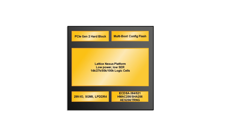
The Lattice MachXO5-NX TDQ devices feature up to 100K logic density, 7.3 Mb internal memory, and 55 Mb dedicated user flash memory. Image used courtesy of Lattice Semiconductor
In-Field Updates and Enhanced Security
The FPGAs also support up to eight Key Authentication Keys and 2,048 Image Signing Keys, with independent revocation and algorithm flexibility. This level of key management provides granular control over device and firmware authentication.
The new MachXO5-NX family extends beyond security to provide enhanced performance and functionality. With logic cell densities reaching up to 100K, the FPGAs offer significant design capacity. The devices feature up to 7.3 Mb of internal memory and 55 Mb of dedicated user flash memory, providing ample storage for configuration and user data.
The devices also support PCIe Gen2 and a variety of I/O voltages, making them suitable for integration into a wide range of systems. The different device selections, such as the LFMXO5-25, LFMXO5-55T, and LFMXO5-100T, offer varying specifications to meet specific application requirements.
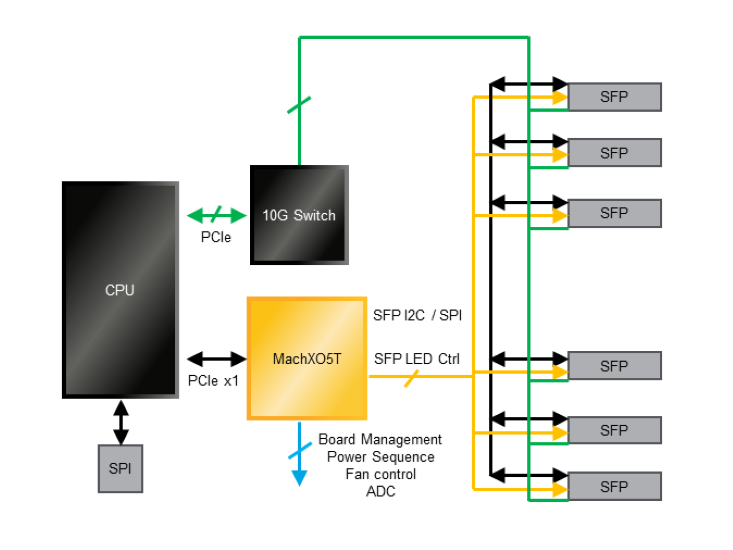
The Lattice MachXO5-NX TDQ in a network switch application. Image used courtesy of Lattice Semiconductor
Secure FPGA Design
The MachXO5-NX TDQ family’s security and performance features make it a viable option for various applications where system control and security are paramount. The devices support the Security Protocol and Data Model 1.4, as well as Hybrid Platform Firmware Resiliency, for robust firmware authentication and recovery. This capability is critical in maintaining system integrity and mitigating supply chain security risks. The hardware-based ML-KEM and LMS-based bitstream authentication further fortify secure channels and ensure the authenticity of the configuration bitstream.
Overall, the MachXO5-NX TDQ is designed to provide a foundational security layer for system management, firmware authentication, and data protection in environments with evolving security requirements. The product family is suitable for use in data centers, industrial automation applications, and communication infrastructure, where protecting sensitive data and ensuring system reliability are critical.


Product OverviewThe REF5030AIDR is a high-precision, low-noise voltage reference IC from Texas Instruments. It is 3 V output with an accuracy of ±0.13%, and it uses an on-chip bandgap architecture to provide a stable reference voltage for demanding applications. The device comes in an 8-pin SOIC package.
Key FeaturesThe REF5030AIDR offers:
Operating ConditionsThe device operates over a temperature range of –40°C to +125°C, making it suitable for industrial and precision applications.
ApplicationsThe REF5030AIDR is ideal for use in: