
Microchip’s SY75714 Bridges 1.2V Cores and Legacy Clock Rails
A four-output buffer converts legacy clock voltages into the sub-2V rails that today's FinFET processors demand, holding jitter to just tens of femtoseconds.
Each generation of FinFET silicon pushes core voltages a little lower, and clock trees have to follow. FPGAs, SoCs, AI accelerators, and the newest CPUs increasingly expect a 1.2V LVCMOS reference at their input pins, yet most board designs still carry clock sources running at 1.8V, 2.5V, or higher. Bridging that gap has traditionally meant resistor dividers or discrete level shifters bolted onto an otherwise clean signal path, components that eat board space and, worse, degrade duty cycle and signal integrity right where precision matters most.
Microchip’s SY75714 tackles that translation problem inside a single package. Part of the broader SY757xx family, the device accepts a supply anywhere from 1.2V to 1.8V and fans a single input reference out to four LVCMOS outputs, each carrying built-in 50-ohm series resistance. That embedded termination lets the outputs drive standard 50-ohm transmission lines directly, sparing engineers from adding external series resistors just to tame reflections. The part is pin-compatible with Texas Instruments’ LMK1C1104, but where that device tops out at a 3.3V rail, the SY75714 was purpose-built for the lower-voltage architectures now common in advanced process nodes.
Timing Performance Worth a Second Look
Clock buffers live or die by how little jitter they add, and the SY75714’s numbers are worth noting. Additive RMS jitter in the 12 kHz to 20 MHz band lands at a typical 16.9 fs when buffering a 156.25 MHz input at 1.8V, climbing to around 36 fs at the lower 1.2V rail, still a small fraction of a picosecond either way. Output-to-output skew stays under 50 ps, and the device-to-device figure tops out at 550 ps, both useful ceilings for designers fanning a single reference out to several downstream loads that need to stay in step. Output turn-on and turn-off are synchronous and require three to five clock cycles to transition, avoiding glitches that can trip up downstream logic during power sequencing or reset events.
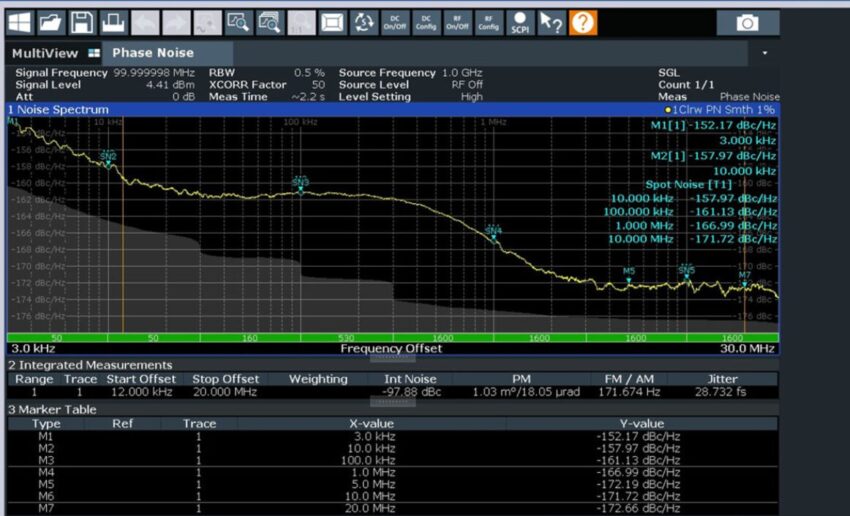
Phase noise plot of the SY75712/SY75714 output clock, showing a noise floor near −171.7 dBc/Hz. Image used courtesy of Microchip
Small Footprint, Wide Operating Range
The SY75714 ships in an 8-pin, 2 mm by 2 mm TDFN package and is rated across an extended −40°C to +105°C range, handling input frequencies from near 0 Hz up to 250 MHz. Supply current scales with rail voltage, running from roughly 6.3 mA at 1.2V up to 9.8 mA at 1.8V under typical conditions, modest figures that suit power-conscious designs without demanding exotic decoupling beyond the standard ferrite-bead-and-capacitor filtering Microchip recommends for the VDD pin.
For engineers laying out clock distribution on next-generation FPGA or SoC boards, the SY75714 removes a recurring headache: getting a legacy-voltage clock source talking cleanly to a low-voltage core without sacrificing jitter performance or burning board space on discrete translation circuitry. Its tight footprint and wide voltage support make it a natural fit for green server designs and battery-powered equipment alike, anywhere a compact, low-jitter fan-out buffer needs to bridge two different clocking worlds without adding noise along the way.


