
IBM Plans Early Nanostack PDK for 3D Transistor Chip Design
A research-stage kit due in the first quarter of 2027 lets fabless firms, tool vendors, and equipment makers test stacked n-type and p-type devices ahead of production.
Stacking transistors vertically, instead of spreading them across a plane, is the central idea behind IBM’s nanostack architecture, and the company now intends to put that idea into designers’ hands. IBM plans to release an early research and development process design kit, or PDK, for the technology in the first quarter of 2027.
The kit accompanies the 0.7 nm (7 angstrom) node that IBM announced earlier this year. By IBM’s account, that node fits nearly 100 billion transistors onto a 150 mm² chip, almost twice the density of the company’s 2 nm node. Projected gains over the earlier node reach up to 50% more performance or up to 70% better energy efficiency, while research on the new structure also shows 40% scaling in SRAM. Production is still a distant prospect; IBM sees a path to manufacturing as early as five years out.
What the First Kit Contains
A PDK bundles the models, design rules, libraries, and other data that engineers need before they can begin laying out chips for a particular manufacturing process. The first nanostack release is expected to include exemplary standard-cell libraries for logic functions, along with an exemplary SRAM design. Armed with those pieces, circuit designers can examine placement and routing, assemble early block-level layouts, and weigh density against power and performance.
Completeness is not the goal at this stage. The initial kit will omit some models that a mature commercial PDK would carry, and its purpose is to seed collaborative research, giving the industry an early chance at design-technology co-optimization while the process is still taking shape. IBM is courting fabless chip companies, electronic design automation (EDA) vendors, equipment suppliers, and research organizations as potential partners.
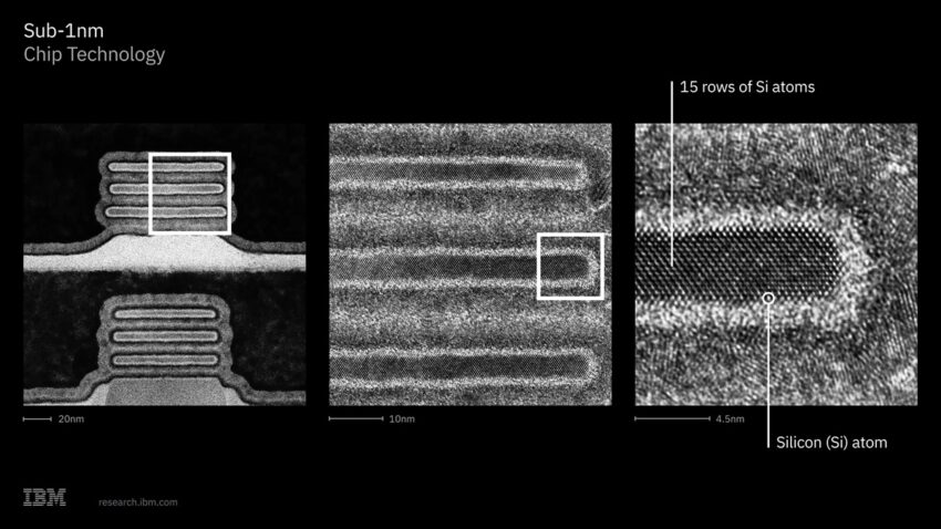
Three zoom levels of IBM’s sub-1nm chip technology, from stacked nanosheet channels (left) down to individual silicon atoms (right). Image used courtesy of IBM
Designing in Three Dimensions
Today’s nanosheet devices place n-type and p-type transistors side by side. Nanostack builds one directly above the other, so circuit layout shifts from two dimensions to three at the transistor level. Separating the pair also lets each device use channel materials tuned to its own behavior, and either polarity can sit on top.
Such freedom carries a price. Stacked devices raise fresh questions about resistance, capacitance, thermal behavior, and interactions between the upper and lower transistors. Fabrication adds hurdles of its own: wafer-to-wafer bonding demands tight control over flatness and alignment, while a thin oxide bonding layer helps hold parasitic capacitance and resistance in check. Wiring grows harder, too, because wires shrink and must span several transistor levels.
Preparing for What Comes Next
Early access gives partners room to act on those questions. EDA vendors can begin adapting their tools to the architecture, equipment makers can study the fabrication challenges its structure creates, and researchers can dig into parasitic extraction, thermal coupling, and device-to-device interactions as the technology matures. The industry has made this kind of leap before, moving from planar transistors to FinFETs and then to nanosheets, and each shift forced a rethink of both manufacturing and design.
In short, the nanostack PDK is a chance to peek at the next chapter of logic scaling before the ink dries. If the projected gains hold up, the payoffs could reach AI training and inference, laptops and phones that last longer between charges, autonomous machines, and monitoring devices that rarely need recharging. Plenty of work still stands between a research kit and shipping silicon, yet it is hard not to wonder what designers will build once they can finally start sketching in the third dimension.


