Auto-Reset – Electronic Circuit Breaker using LT1153
This project is a precise, low-cost electronic circuit breaker based on the LT1153 chip and an N-channel MOSFET. It protects loads by tripping for ∼200ms and then auto-resetting until the fault clears. The trip current, delay, and auto-reset period are fully programmable.
This project is a precise, low-cost electronic circuit breaker designed to protect sensitive loads from over-current conditions. When an over-current event occurs, the breaker trips for approximately 200 ms and then automatically resets. This cycle continues until the fault is cleared, ensuring reliable protection for both the load and the MOSFET switch.
The trip current, trip delay time, and auto-reset period are fully programmable over a wide range, making the design suitable for various load impedance. An active-high shutdown input is provided, which can be connected directly to a PTC thermistor to enable thermal protection. An open-drain status output is included for interfacing with a microcontroller to report fault conditions.
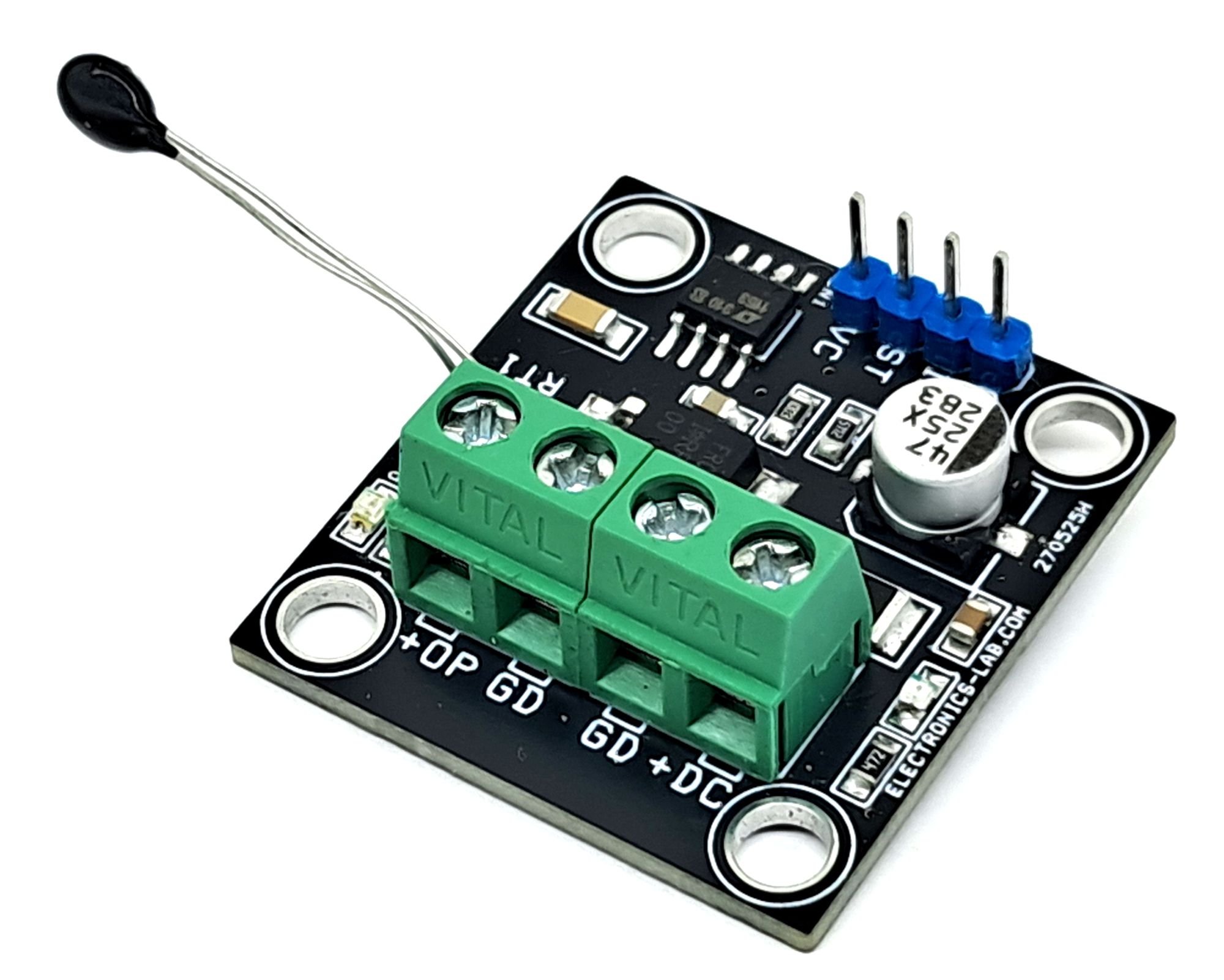
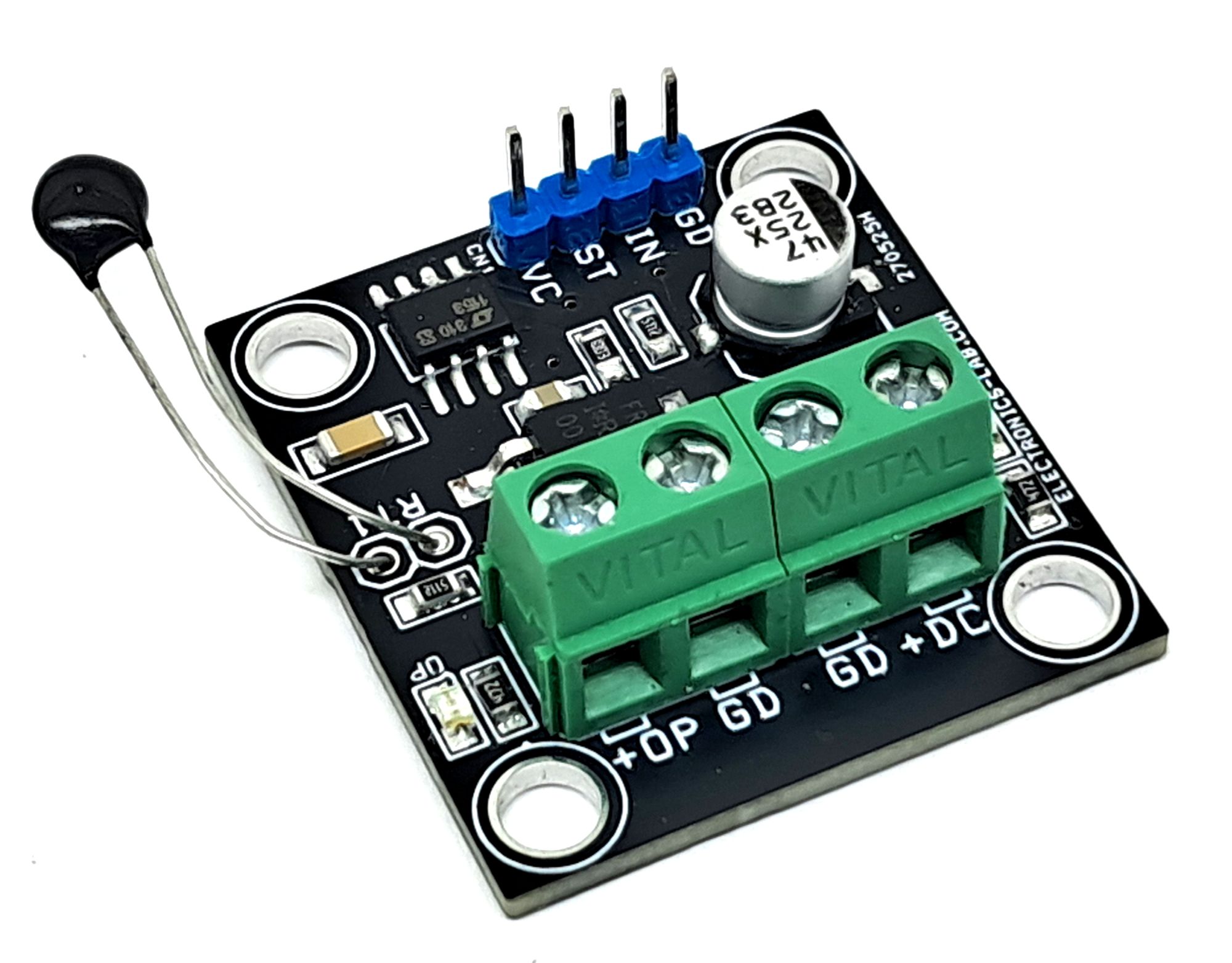
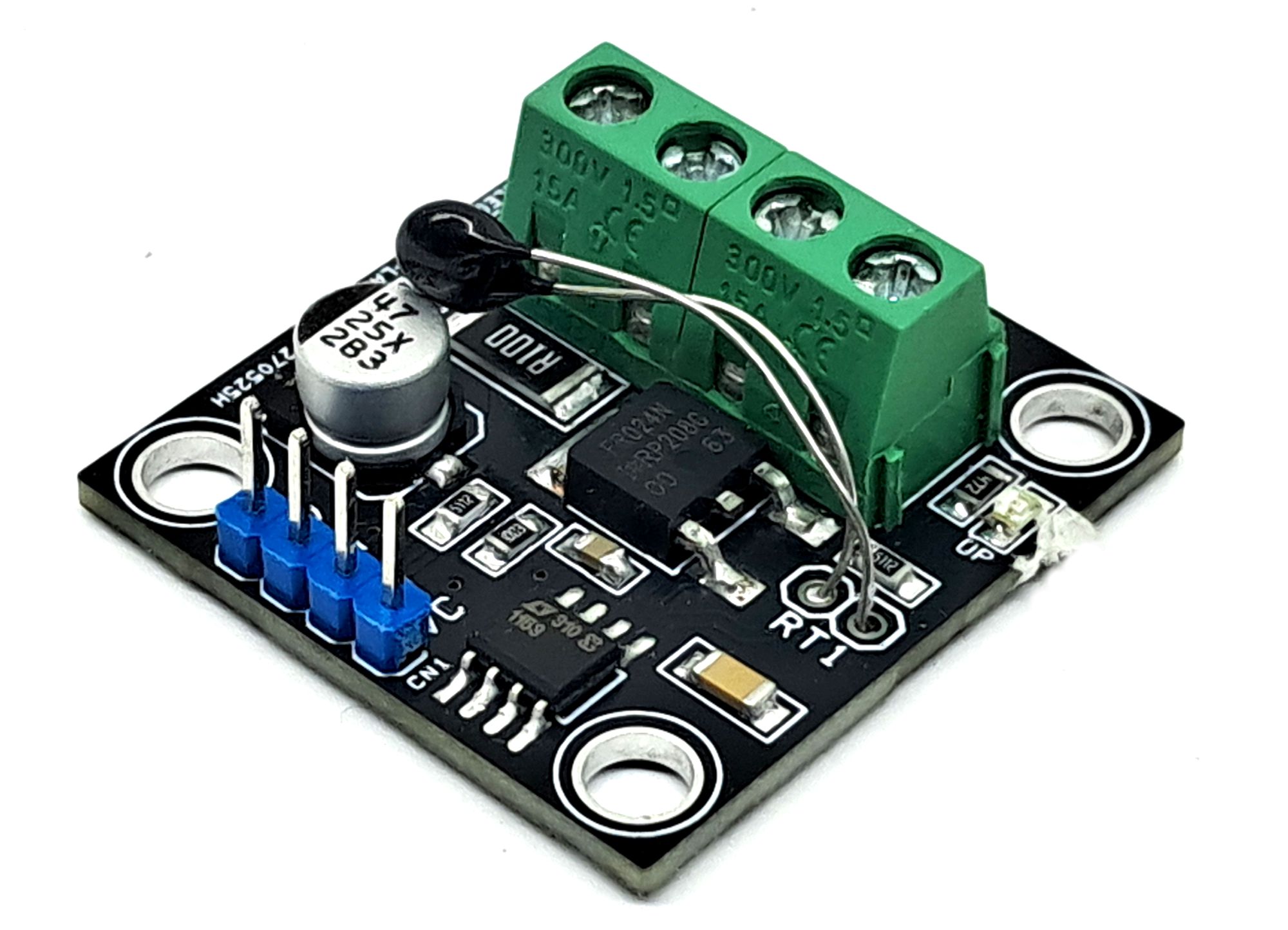
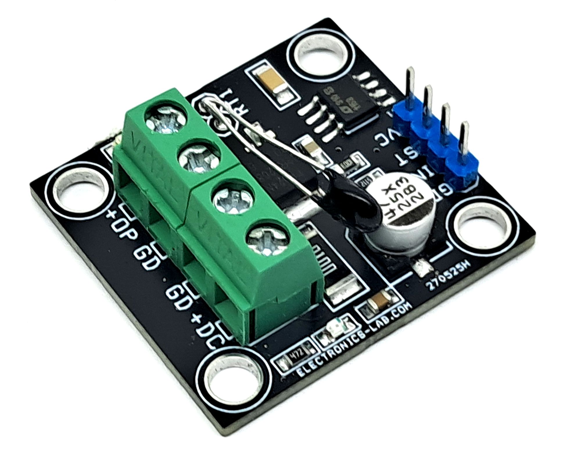
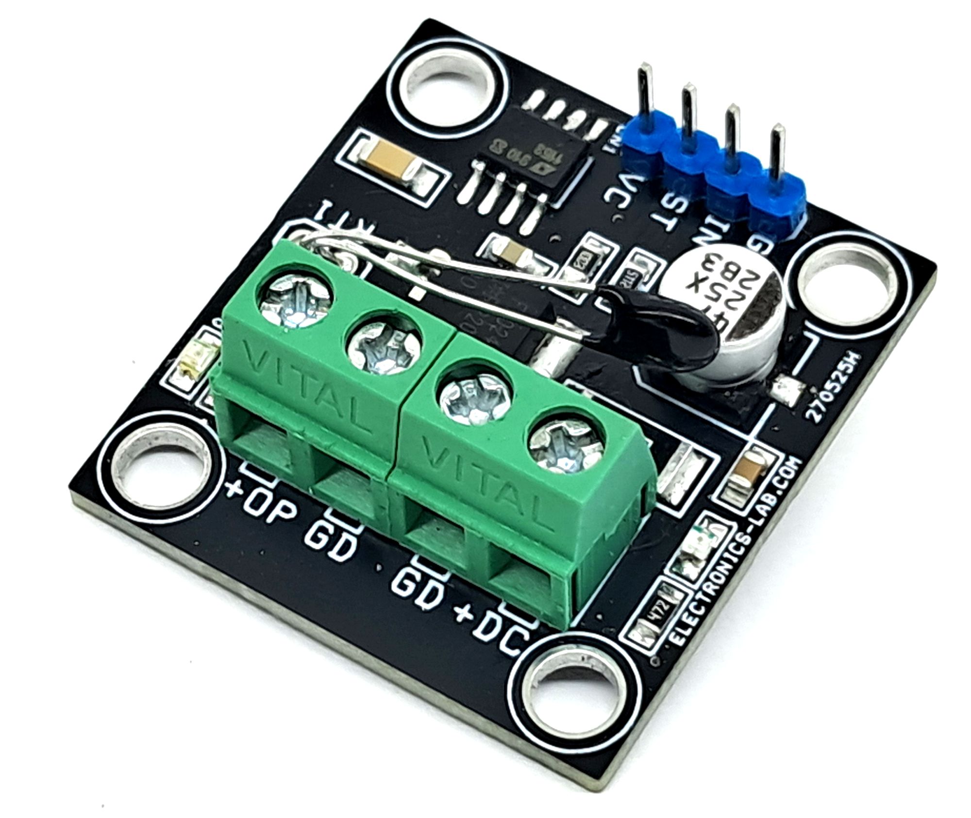
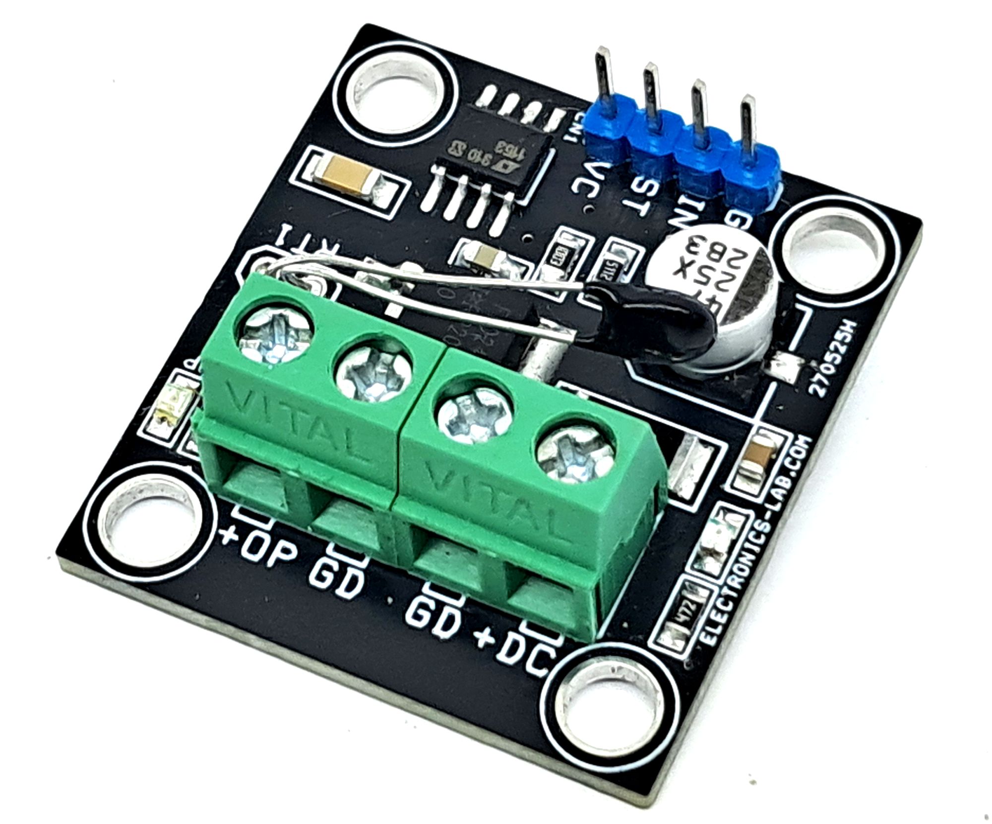
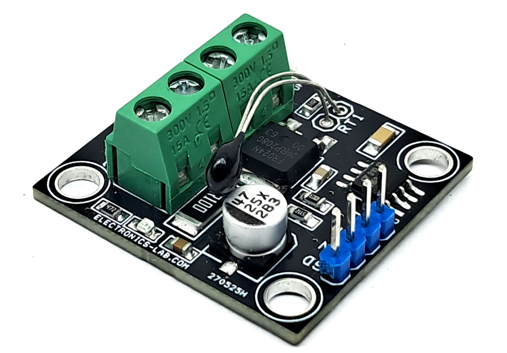
The project uses the LT1153 chip along with an N-channel MOSFET for driving the output load. Power indication is provided through separate input and output LEDs, and screw terminals are included for easy input and output connections.
Key Features
- Programmable Auto-Reset Time: 1 mS to over 10 s
(Capacitor C4 determines the auto-restart time; refer to the LT1153 datasheet for more details.) - Programmable Trip Delay: 15 µs to over 100 mS
(Set using C2 and R3.) - Programmable Trip Current: 1 mA to over 20 A
(Set using sense resistor R2 and selecting an appropriate MOSFET based on load requirements.) - Fault Status Output: Open-drain output indicates fault condition.
- RT1 (PTC): Provides over-temperature protection.
Specifications
- Input Supply: 5 V DC
- Output Supply: 5 V DC
- Maximum Load Current: 1 A
- Trip Delay: 1 ms
- Temperature Sensor Optional (Trip Point 70 Degree C)
- Auto-Reset Period: 200 ms
- D2: Output power LED
- D1: Input power LED
- PCB Dimensions: 33.66 x 31.12 mm
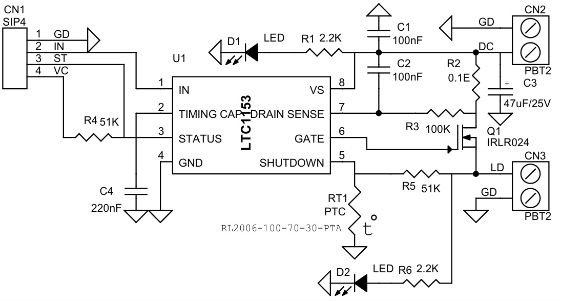
Timing Capacitor C4 Pin (Auto-Reset Timer) The small capacitor charging current (4.2µA) produces large delays with relatively small valued capacitors, but care must be taken to ensure that this current is not shunted to ground through a leaky capacitor or printed circuit board trace. The timing capacitor voltage is sensed by a high impedance CMOS comparator input with ESD clamp diodes to ground and supply and therefore should not be forced beyond the power supply rails. This pin can be grounded if the auto-reset function is not used.
Input and Shutdown Pins the LTC1153 input pin is active high and activates all of the protection and charge pump circuitry when switched ON. The shutdown pin is designed to break the circuit if a secondary fault condition (over temperature, etc.) is detected. The LTC1153 logic and shutdown inputs are high impedance CMOS gates with ESD protection diodes to ground and supply and therefore should not be forced beyond the power supply rails. The shutdown pin should be connected to ground when not in use
Status Pin The status pin is an open-drain output which is driven low whenever the breaker is tripped. A 51k pull-up resistor should be connected between this output and a logic supply. The status pins of multiple LTC1153s can be OR’d together if independent fault sensing is not required. No connection is required to this pin when not in use.
Drain Sense Pin (Trip Delay Capacitor C2 and Resistor R3) The drain sense pin is compared against the supply pin voltage. If the voltage at this pin is more than 100mV below the supply pin, the input latch will trip and the MOSFET switch will be turned off. This pin is also a high impedance CMOS gate with ESD protection and therefore should not be forced beyond the power supply rails. Some loads, such as large supply capacitor, lamps, or motors require high inrush currents. An RC time is added between the sense resistor and the drain sense pin to ensure that the drain sense circuitry does not false trigger during start-up. This trip delay can be set from a few microseconds to many seconds. However, very long de lays may put the MOSFET switch in risk of being destroyed by a short-circuit condition. (see Applications Information Section).
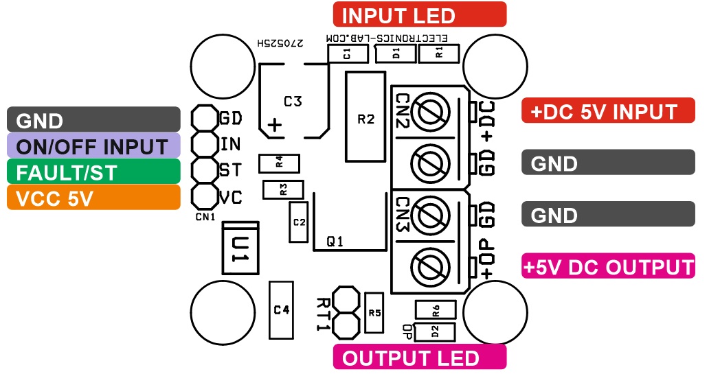
Connections
- CN1: Pin 1 = GND, Pin 2 = Load ON/OFF, Pin 3 = Status Output (Normally High), Pin 4 = 5V For Status Pin Pull Up
- CN2: Pin 1 = GND, Pin 2 = Input Supply
- CN3: Pin 1 = + Load, Pin 2 = GND
- D1: Input Power LED
- D2: Output Power LED
Schematic
Parts List
| NO | QNTY. | REF. | DESC. | MANUFACTURER | SUPPLIER | SUPPLIER PART NO |
|---|---|---|---|---|---|---|
| 1 | 1 | CN1 | 4 PIN MALE HEADER PITCH 2.54MM | WURTH | DIGIKEY | 732-5317-ND |
| 2 | 2 | CN2,CN3 | 2 PIN SCREW TERMINAL PITCH 5.08MM | SCREW TERMINAL | DIGIKEY | |
| 3 | 1 | C4 | 220nF/25V CERAMIC SMD SIZE 1206 | YAGEO/MURATA | DIGIKEY | |
| 4 | 2 | C1,C2 | 100nF/25V CERAMIC SMD SIZE 0805 | YAGEO/MURATA | DIGIKEY | |
| 5 | 1 | C3 | 47uF/25V ELECTROLYTIC | PANASONIC | DIGIKEY | PCE3804CT-ND |
| 6 | 2 | D1,D2 | LED RED SMD SIZE 0805 | OSRAM | DIGIKEY | 475-1278-1-ND |
| 7 | 1 | Q1 | IRLR024 SMD PAK | VISHAY | DIGIKEY | IRLR024-ND |
| 8 | 1 | RT1 | PTC THERMISTER 150OHM OPTIONAL | AMPHENOL | DIGIKEY | |
| 9 | 2 | R1,R6 | 2.2K 5% SMD SIZE 0805 | YAGEO/MURATA | DIGIKEY | |
| 10 | 1 | R2 | 0.1E/2W 1% SMD SIZE 2512 | BOURNS INC | DIGIKEY | CRA2512-FZ-R100ELFCT-ND |
| 11 | 1 | R3 | 100K 5% SMD SIZE 0805 | YAGEO/MURATA | DIGIKEY | |
| 12 | 2 | R4,R5 | 51K 1% SMD SIZE 0805 | YAGEO/MURATA | DIGIKEY | |
| 13 | 1 | U1 | LTC1153 SMD SOIC8 | ANALOG DEVICE | DIGIKEY | LTC1153IS8#PBF-ND |
Connections
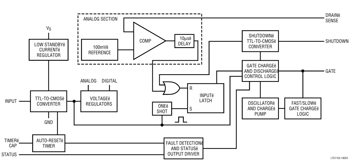
LT1153 Block Diagram
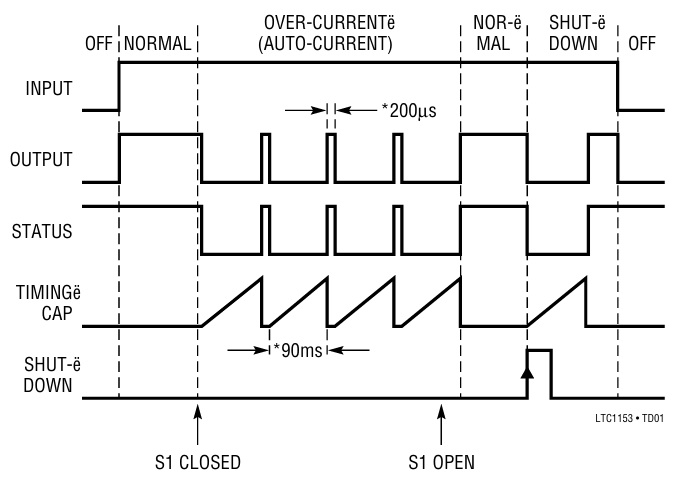
Timing Diagram
Gerber View
Photos