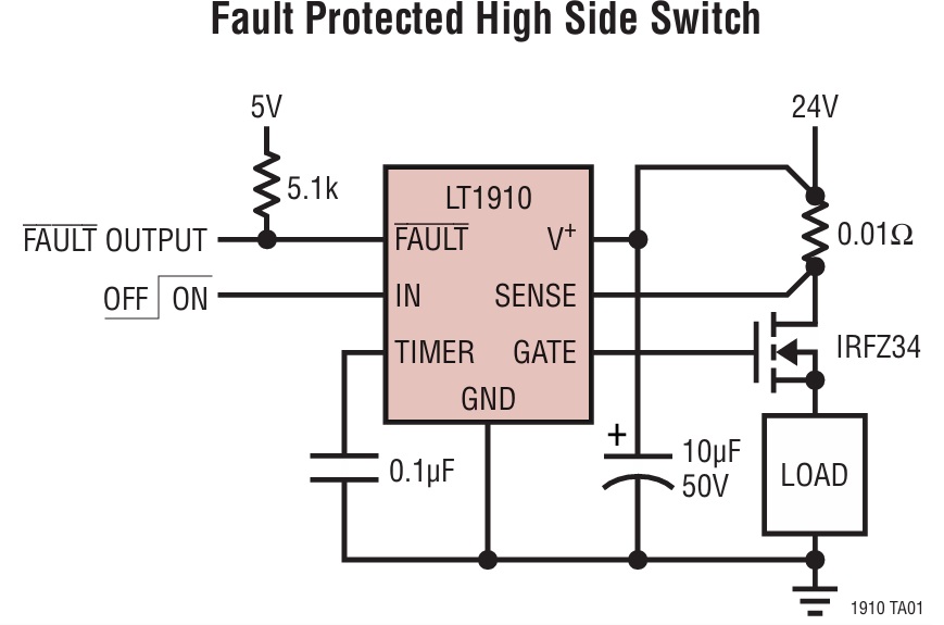
Fault Protected High Side Switch
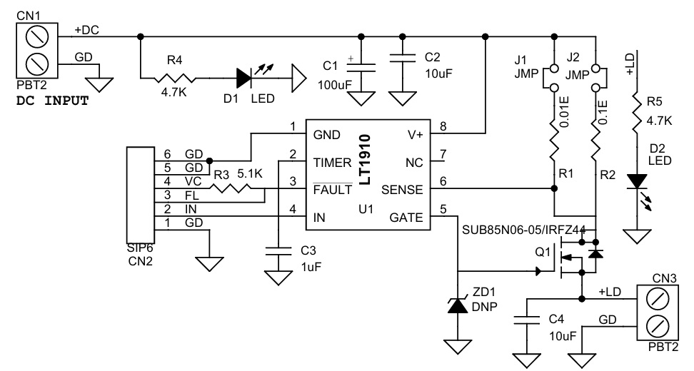
This project uses the LT1910 high-side switch to protect a load from over-current. It automatically shuts off, flags the fault, waits 150 ms, and attempts to restart. The current trip point is set via selectable shunt resistors.
This project is designed to protect the load from over-current conditions using the LT1910 fault-protected high-side switch controller. When the internal drain comparator detects that the switch current exceeds the preset threshold, the LT1910 immediately turns off the switch and asserts a fault flag.
The switch remains off for approximately 150 ms, as determined by the external timing capacitor C3, and then automatically attempts to restart. If the fault condition persists, the protection cycle repeats until the fault is cleared, thereby safeguarding the MOSFET and the load. Once the switch restarts successfully, the fault flag is reset.
The LT1910 features a 50-mV trip point for current sensing, which determines the value of the shunt resistor. The board includes two selectable shunt resistor options — 0.01 Ω and 0.1 Ω — which can be configured using jumpers J1 and J2. A third option allows both shunt resistors to be used in parallel (by closing both jumpers J1 and J2), providing additional flexibility in setting the desired trip point.
Features
- 12V to 24V Power Supply Range
- Protected from –15V to 60V Supply Transients
- Short-Circuit Protected
- VCC 5V for Fault Pull-Up
- Automatic Restart Timer Approx 150mS
- Open-Collector Fault Flag with Pull Up, Normally High
- Fully Enhances N-Channel MOSFET Switches
- Programmable Current Limit, Delay Time and Auto Restart Period
- Voltage Limited Gate Drive
- Defaults to Off State with Open Input
- Turn On Time 75uS
- Turn Off Time 10uS
- Maximum Output Current Shunt Resistor 0.1 Ohm, Current 0.6A
- Maximum Output Current Shunt Resistor 0.01 Ohm, 6A
- 4 x 4 mm Mounting Holes
- PCB Dimensions 42.55 x 35.56 mm
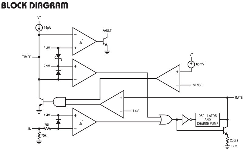
The LT1910 is a high side gate driver that allows the use of low-cost N-channel power MOSFETs for high side switching applications. It contains a completely self-contained charge pump to fully enhance an N-channel MOSFET switch with no external components. The LT1910 has been specifically designed for harsh operating environments such as industrial, avionics and automotive applications where poor supply regulation and/or transients may be present. The device will not sustain damage from supply transients of –15V to 60V.
FAULT (Pin 3): The FAULT pin monitors the TIMER pin voltage and indicates the overcurrent condition. Whenever the TIMER pin is pulled below 3.3V at the onset of a current limit condition, the FAULT pin pulls active LOW. The FAULT pin resets HIGH immediately when the TIMER pin ramps above 3.4V during auto restart. The FAULT pin is an open-collector output, thus requiring an external pull-up resistor and is intended for logic interface. The resistor should be selected with a maximum of 1mA pull-up at low status.
IN (Pin 4): The IN-pin threshold is TTL/CMOS compatible and has approximately 200mV of hysteresis. When the IN pin is pulled active HIGH above 2V, an internal charge pump is activated to pull up the GATE pin. The IN pin can be pulled as high as 15V regardless of whether the supply is on or off. If the IN pin is left open, an internal 75k pull-down resistor pulls the pin below 0.8V to ensure that the GATE pin is inactive LOW
TIMER (Pin 2): A timing capacitor, CT , from the TIMER pin to ground sets the restart time following overcurrent detection. Upon detection of an overcurrent condition, CT is rapidly discharged to less than 1V and then recharged by a 14µA nominal current source back to the 2.9V timer threshold, whereupon the restart is attempted. Whenever TIMER pulls below 2.9V, the GATE pin pulls low to turn off the external switch. This cycle repeats until the overcurrent condition goes away and the switch restarts successfully. During normal operation the pin clamps at 3.5V nominal.
The LT1910 GATE pin has two states, off and on. In the off state it is held LOW, while in the on state it is pumped to 12V above the supply by a self-contained 750kHz charge pump. The off state is activated when either the IN pin is below 0.8V or the TIMER pin is below 2.9V. Conversely, for the on state to be activated, the IN pin must be above 2V and the TIMER pin must be above 2.9V. The IN pin has approximately 200mV of hysteresis. If it is left open, the IN pin is held LOW by a 75k resistor. Under normal conditions, the TIMER pin is held a diode drop above 2.9V by a 14µA pull-up current source. Thus, the TIMER pin automatically reverts the GATE pin to the on state if the IN pin is above 2V.
The SENSE pin normally connects to the drain of the power MOSFET, which returns through a low value drain-sense resistor to supply. In order for the sense comparator to accurately sense the MOSFET drain current, the V+ pin must be connected directly to the positive side of the drain-sense resistor. When the GATE pin is on and the MOSFET drain current exceeds the level required to generate a 65mV drop across the drain-sense resistor, the sense comparator activates a pull-down NPN which rapidly pulls the TIMER pin below 2.9V. This in turn causes the timer comparator to override the IN pin and set the GATE pin to the off state, thus protecting the power MOSFET. When the TIMER pin is pulled below 3.3V, the fault comparator also activates the open-collector NPN to pull the FAULT pin LOW, indicating an overcurrent condition. When the MOSFET gate voltage is discharged to less than 1.4V, the TIMER pin is released. The 14µA current source then slowly charges the timing capacitor back to 2.9V where the charge pump again starts to drive the GATE pin HIGH. If a fault condition still exists, the sense comparator threshold will again be exceeded and the timer cycle will repeat until the fault is removed. The FAULT pin becomes inactive HIGH if the TIMER pin charges up successfully above 3.4V
Automatic Restart Period The timing capacitor, CT, determines the length of time the power MOSFET is held off following a current limit trip. Curves are given in the Typical Performance Characteristics to show the restart period for various values of CT. For example, C3/CT = 1µF yields a 150ms restart period and 0.33uF 50mS.
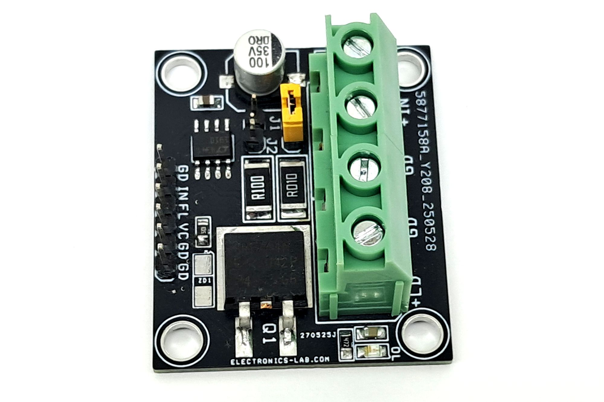
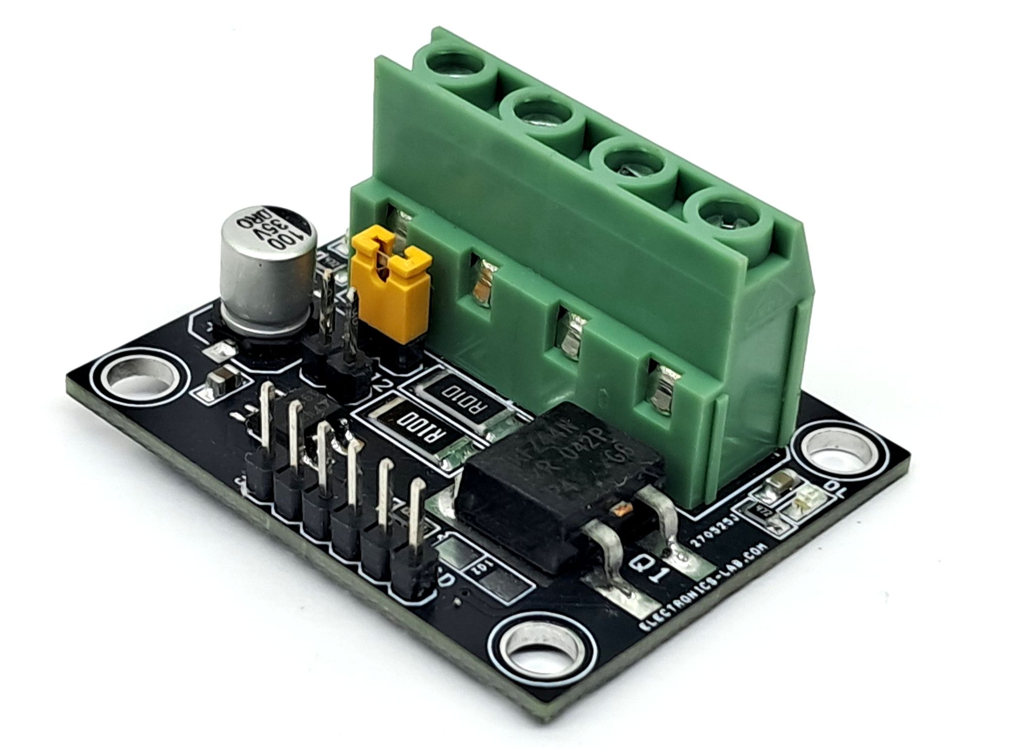
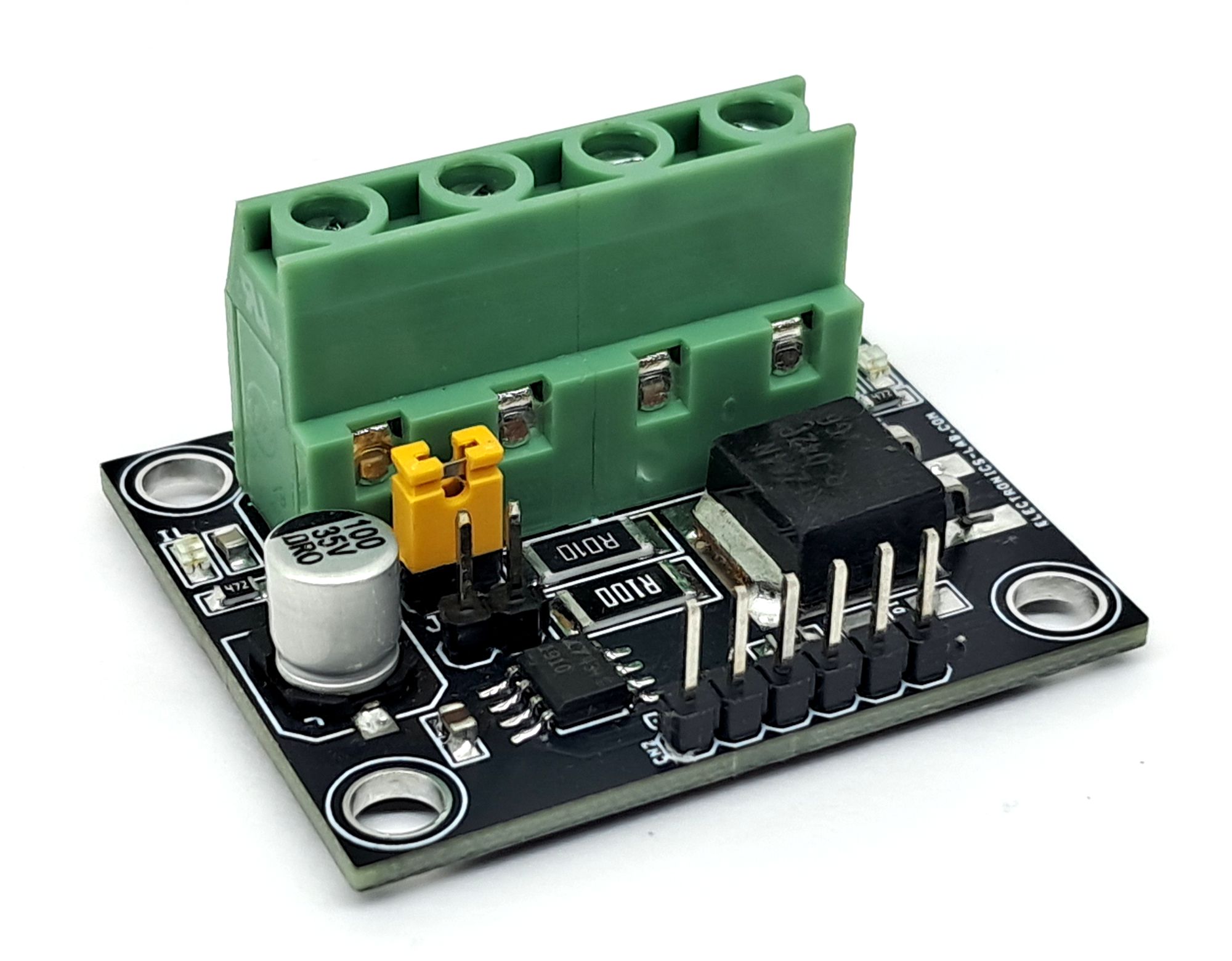
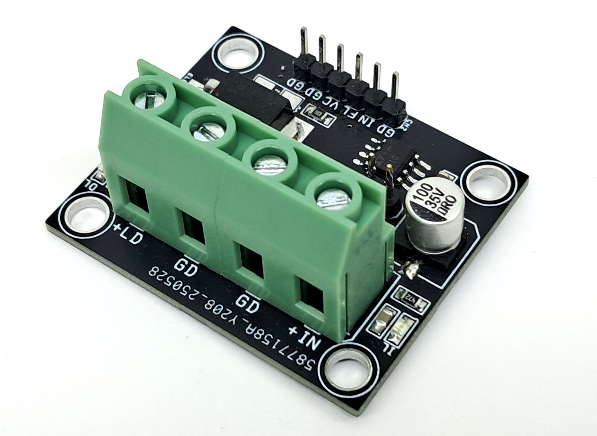
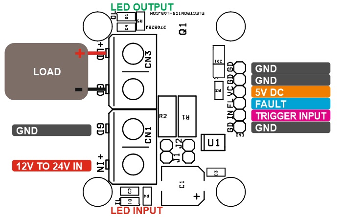
Connections
- CN1: Pin 1 = +Load Power Input 24V DC, Pin 2 = GND
- CN2: Pin 1 = GND, Pin 2 = Trigger Input 5V, Pin 3 = Fault Output Normally High, Pin 4 = VCC 5V DC, Pin 5 GND, Pin 6 = GND
- CN3: Pin 1 = +Load, Pin 2 = GND
- J1: Jumper for Low Current Range
- J2: Jumper for High Current Range
- D1: Input Power LED
- D2: Output LED
Schematic
Parts List
| NO. | QNTY. | REF. | DESC. | MANUFACTURER | SUPPLIER | SUPPLIER PART NO |
|---|---|---|---|---|---|---|
| 1 | 2 | CN1,CN3 | 2 PIN SCREW TERMINAL PITCH 7.62MM | PHOENIX | DIGIKEY | 277-5849-ND |
| 2 | 1 | CN2 | 6 PIN MALE HEADER PITCH 2.54MM | WURTH | DIGIKEY | 732-5319-ND |
| 3 | 1 | C1 | 100uF/35V ELECTROLYTIC | NICHICOM | DIGIKEY | 493-2203-1-ND |
| 4 | 2 | C2,C4 | 10uF/35V CERAMIC SMD SIZE 0805 | DIGIKEY | ||
| 5 | 1 | C3 | 1uF/35V CERAMIC SMD SIZE 0805 | DIGIKEY | ||
| 6 | 2 | D1,D2 | LED RED SMD SIZE 0805 | OSRAM | DIGIKEY | 475-1278-1-ND |
| 7 | 2 | J1,J2 | 2 HEADER PITCH 2.54MM FOR JUMPER J1/J2 | WURTH | DIGIKEY | 732-5315-ND |
| 8 | 1 | Q1 | SUB85N06-05/IRFZ44 | INFINEON | DIGIKEY | IRFZ44NSTRLPBFCT-ND |
| 9 | 1 | R1 | 0.01E/2W 1% SMD SIZE 2512 | BOURNS INC | DIGIKEY | CRF2512-FZ-R010ELFCT-ND |
| 10 | 1 | R2 | 0.1E/2W 1% SMD SIZE 2512 | BOURNS INC | DIGIKEY | CRM2512-FX-R100ELFCT-ND |
| 11 | 1 | R3 | 5.1K 1% SMD SIZE 0805 | DIGIKEY | ||
| 12 | 2 | R4,R5 | 4.7K 5% SMD SIZE 0805 | DIGIKEY | ||
| 13 | 1 | U1 | LT1910 | ANALOG DEVICE | DIGIKEY | 505-LT1910ES8#TRPBFCT-ND |
| 14 | 1 | ZD1 | DNP | DIGIKEY | ||
| 15 | 1 | SHUNT | SHUNT FOR JUMPER J1 OR J2 | SULINS CONNECT | DIGIKEY | S9001-ND |
Connections
Chip Block Diagram
Application Schematic
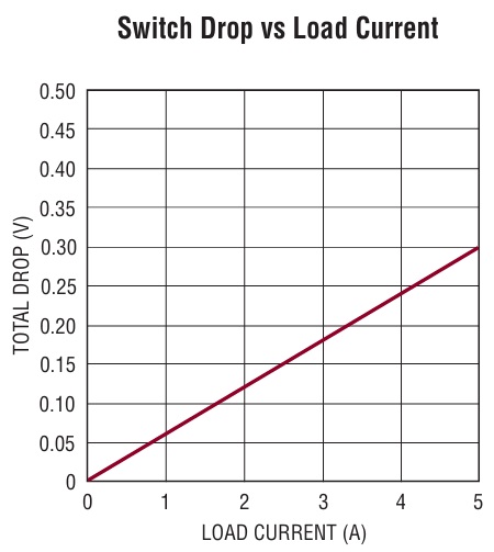
Voltage Drop vs Load Current
Gerber View
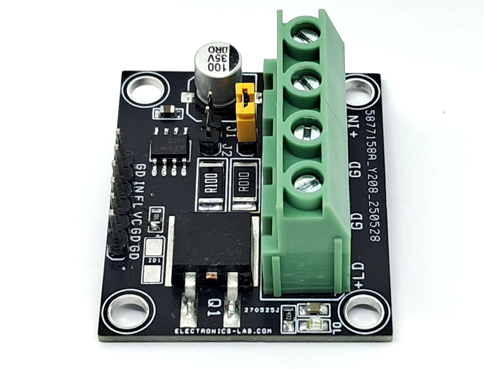
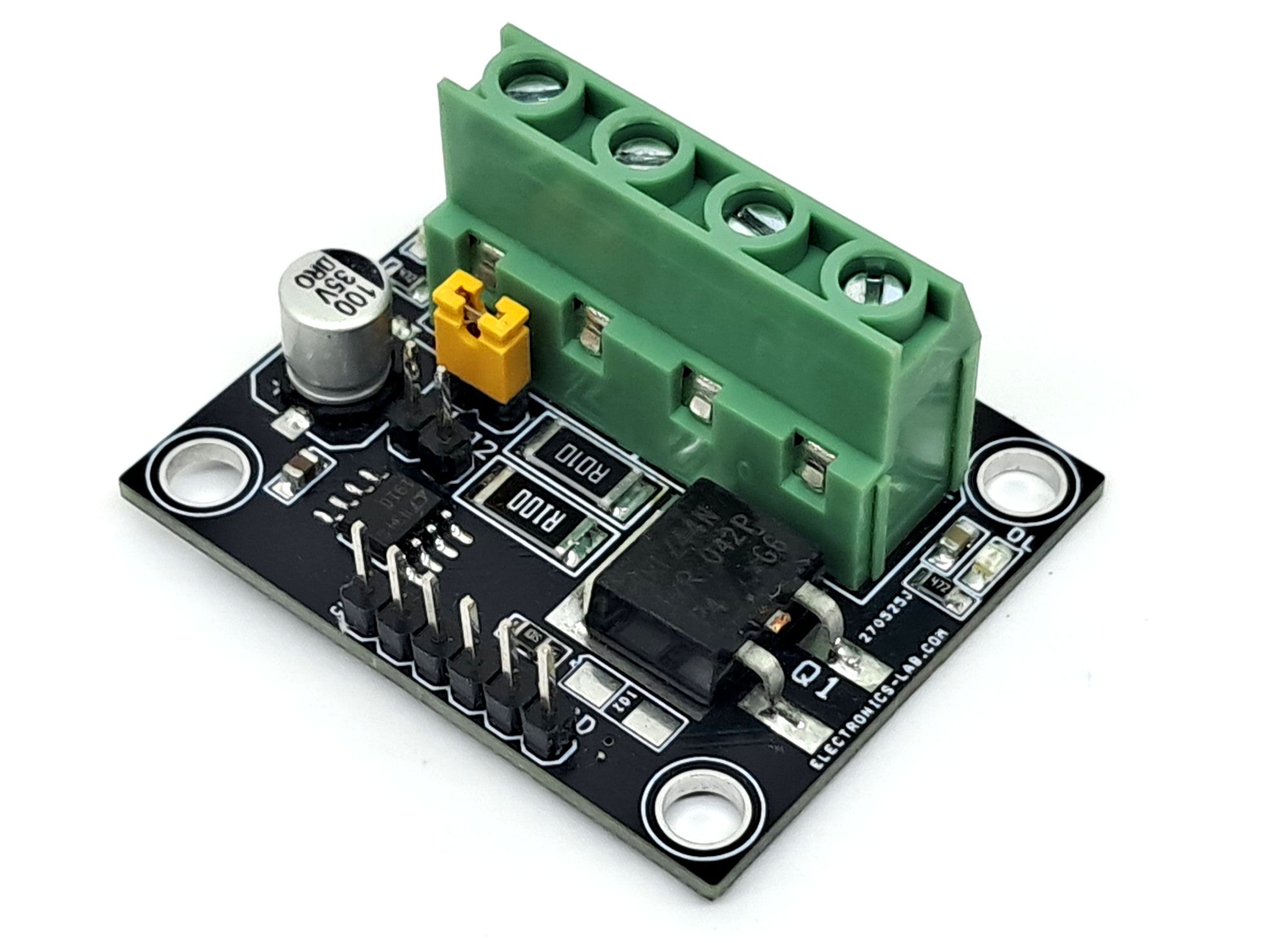
Photos