High Voltage SiC-MOSFET Switch with Isolated Gate Driver and Isolated DC-DC Converter
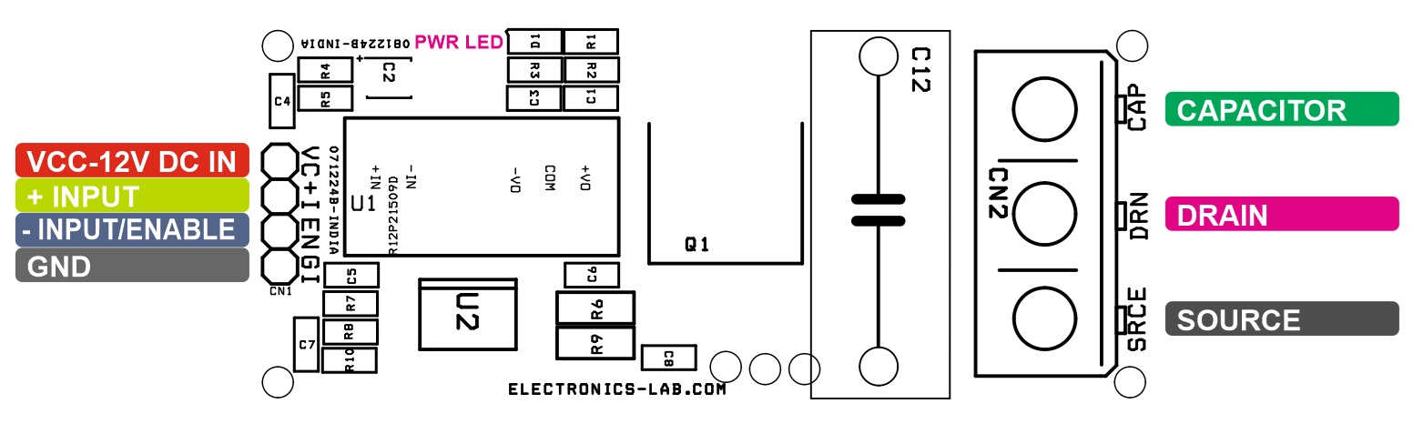
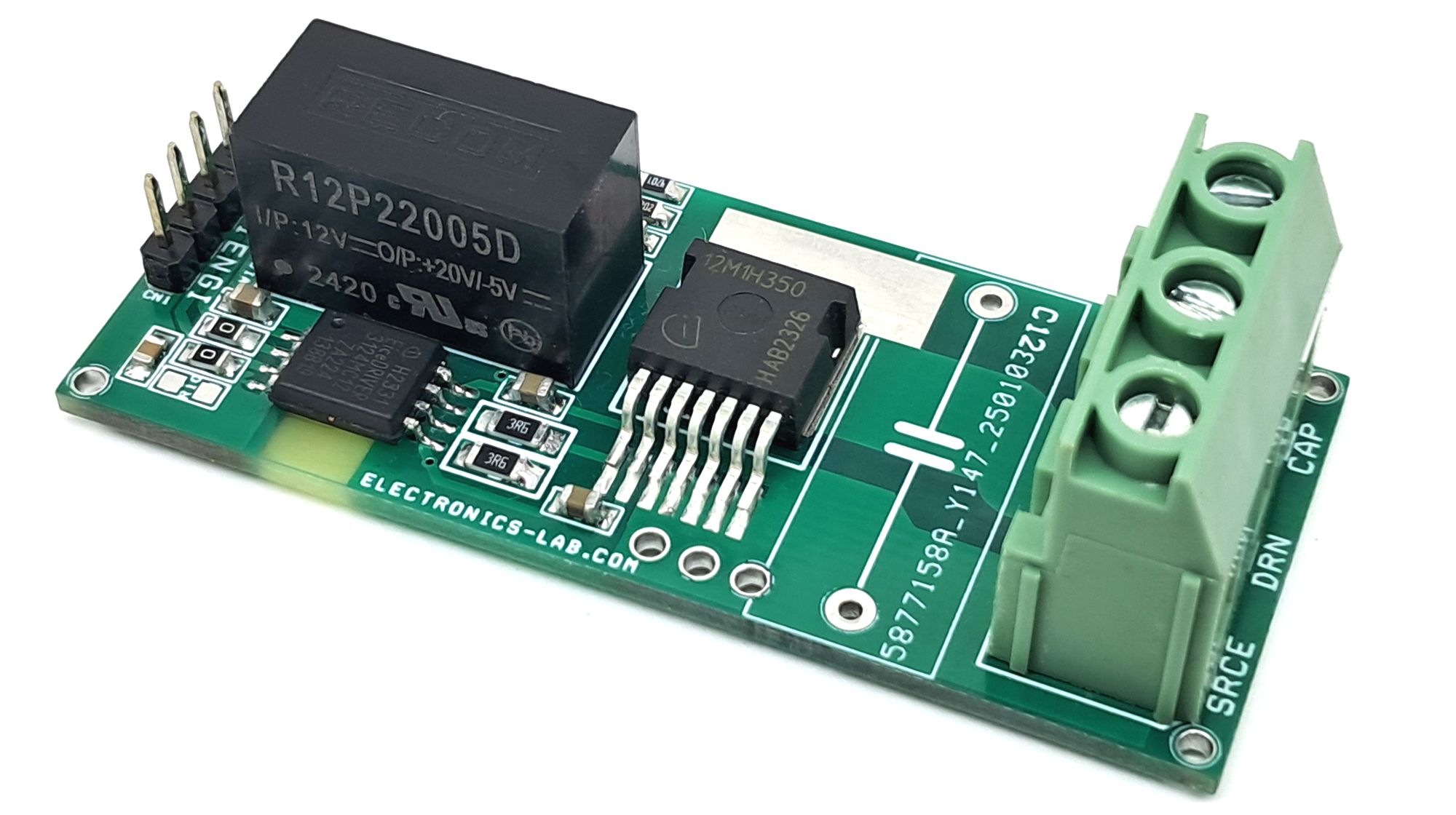
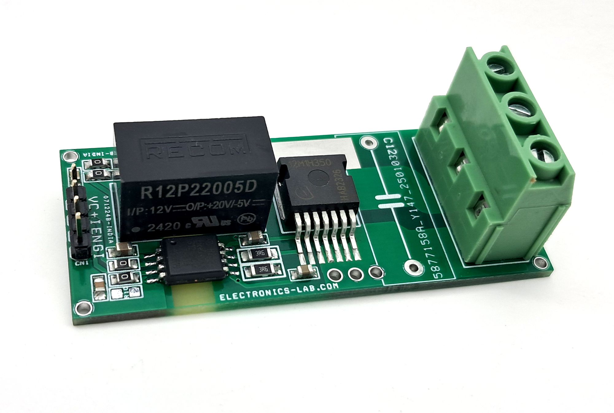
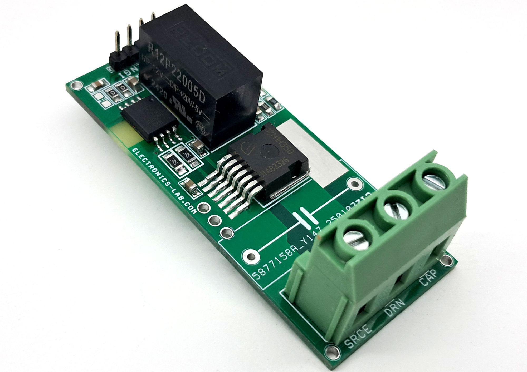
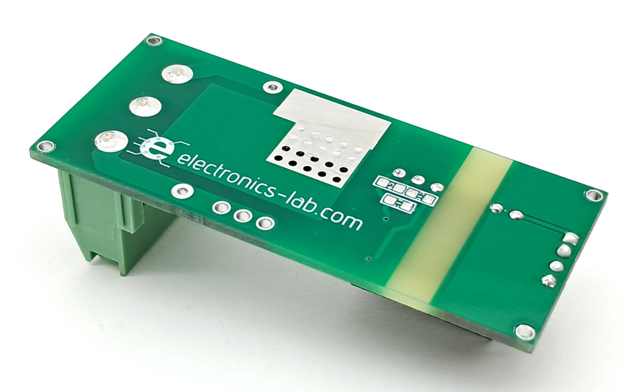
The isolated high-voltage SiC MOSFET switch is a reliable and efficient solution for power driver applications. It includes a gate driver chip, a 1.2kV/4.7A SiC MOSFET, and a 2W DC-DC converter. The module is suitable for various configurations and can be connected to high-current/voltage screw terminals.
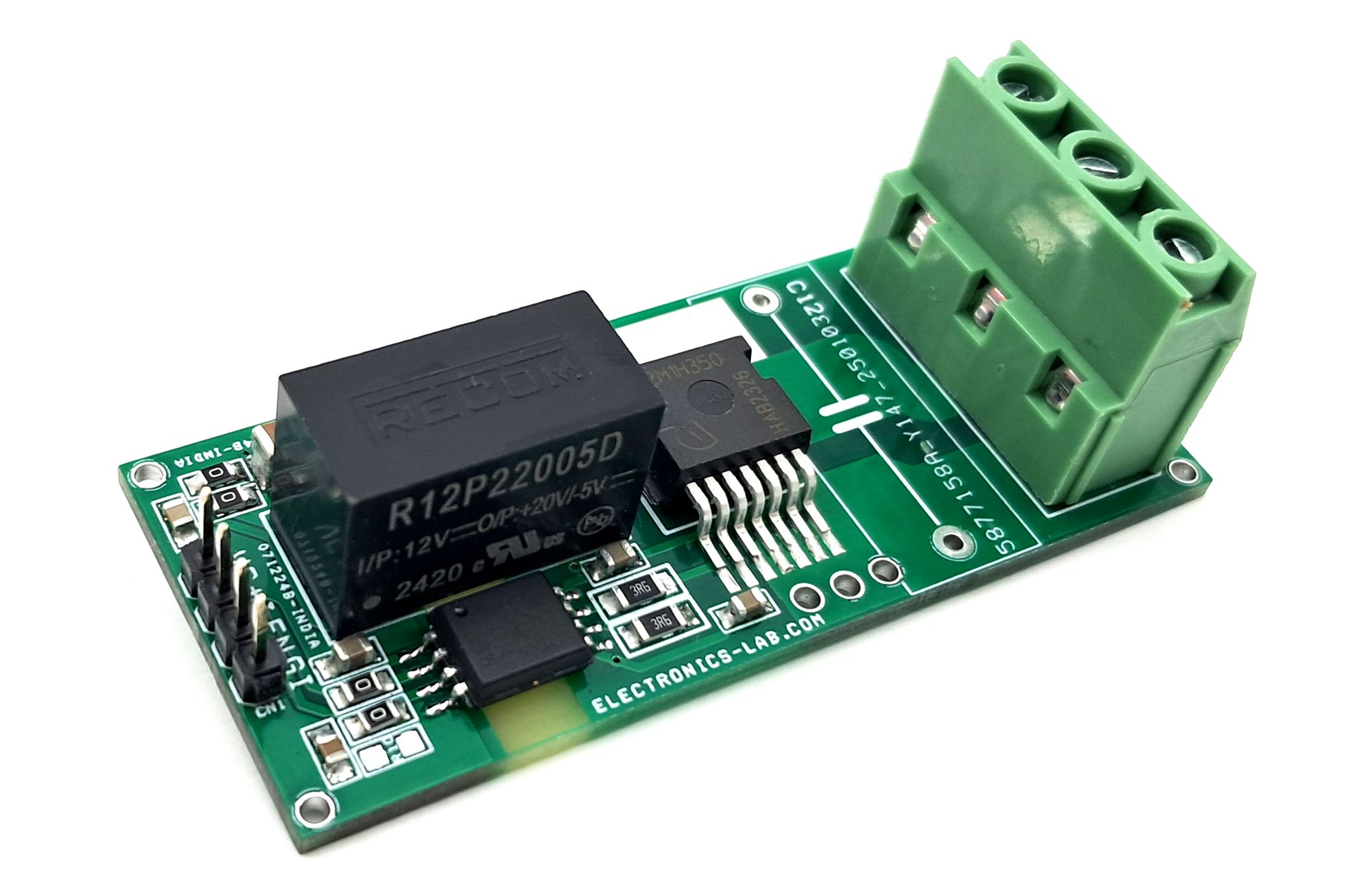
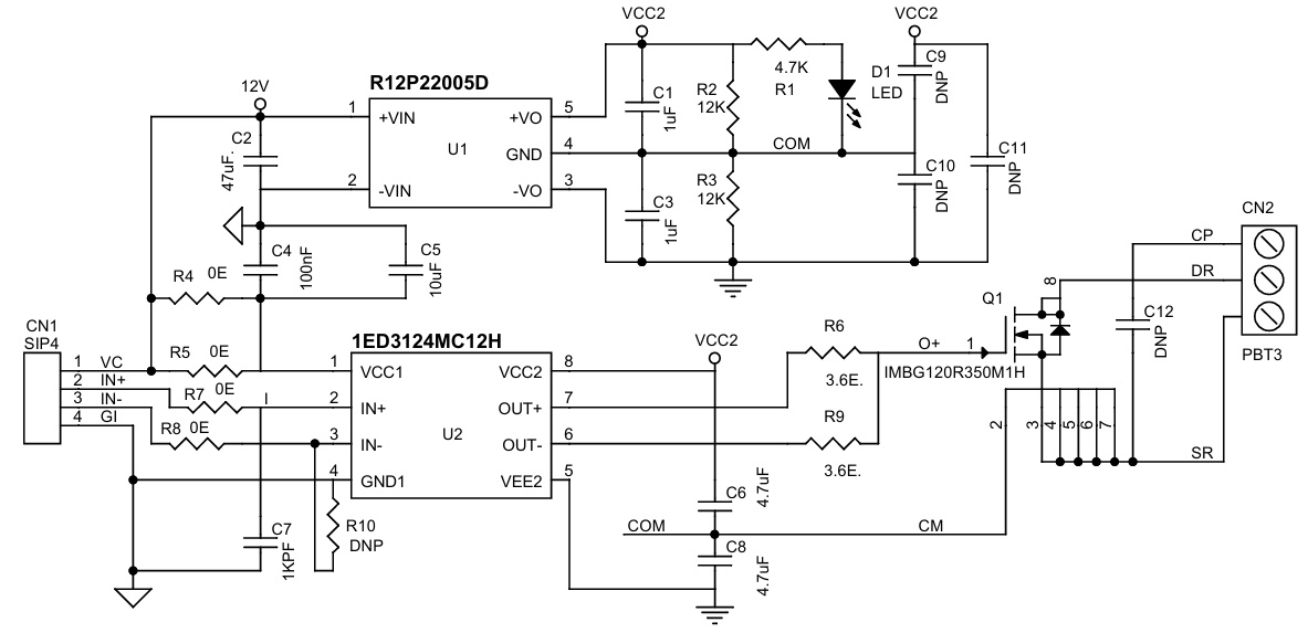
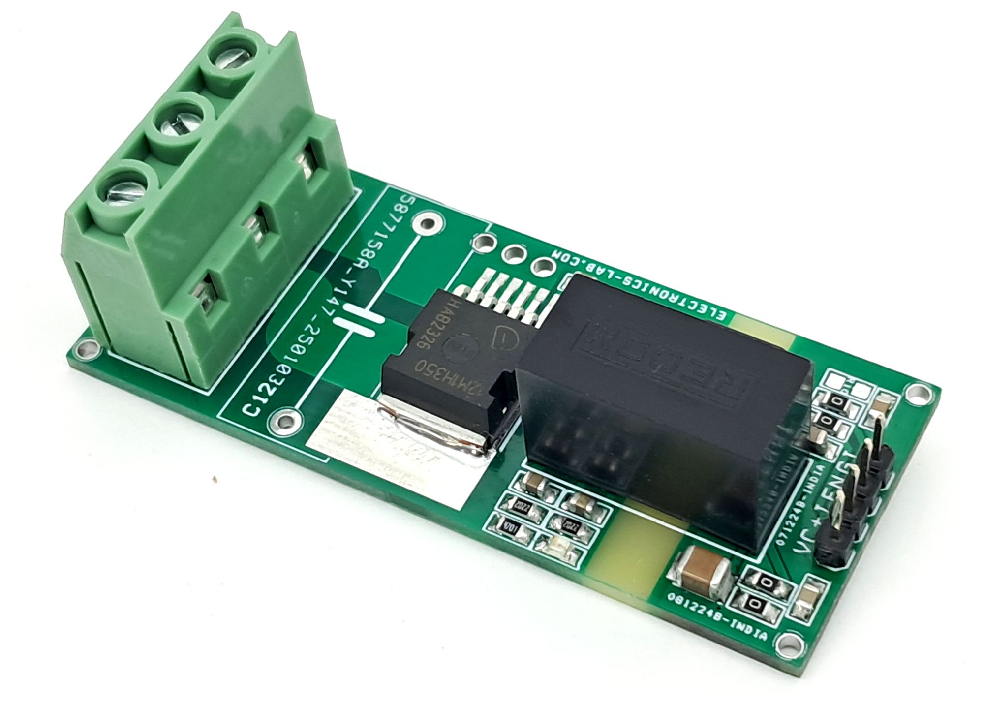
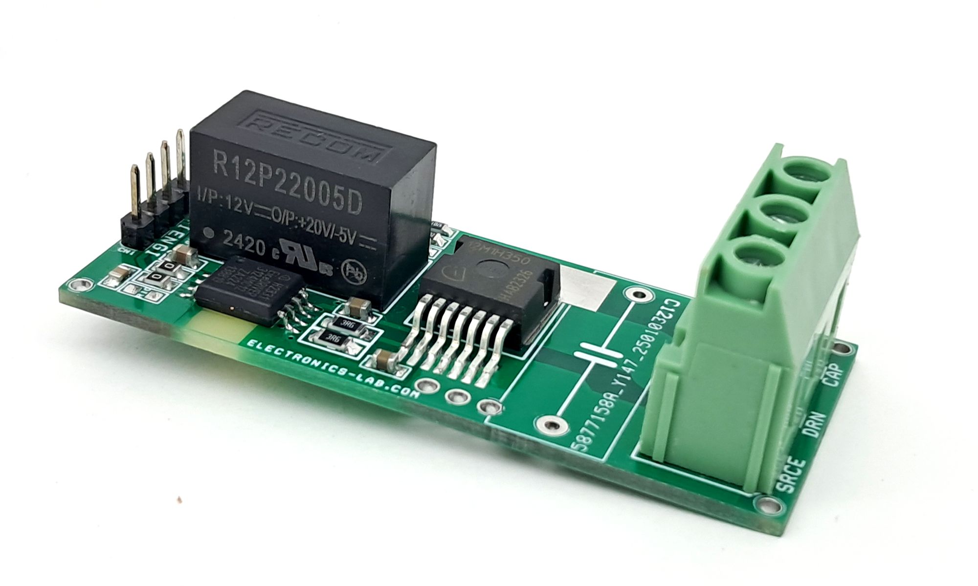
The isolated high-voltage SiC MOSFET switch offers a straightforward solution for power drivers, comprising a gate driver chip (1ED3124MC12H), a 1.2kV/4.7A SiC MOSFET, and an isolated 2W DC-DC converter (R12P22005D). The gate driver chip is optimized for high-frequency operations and can deliver high gate driver currents of up to 14A. This module is well-suited for various applications, including half-bridge, full-bridge, and single SiC MOSFET switch configurations.
For convenient access, the Source and Drain of the SiC MOSFET are connected to high-current/voltage screw terminals. Additionally, an optional high-voltage C12 capacitor can be installed as per the specific application requirements, providing flexibility and adaptability to different use cases. Overall, this isolated high-voltage SiC MOSFET switch module provides a reliable and efficient solution for power driver applications.
Logic input: to output switching behavior There are two possible input modes to control the SiC MOSFET. At non-inverting mode IN+ controls the driver output while IN- is set to low. At inverting mode IN- controls the driver output while IN+ is set to high. A minimum input pulse width is defined to filter occasional glitches.
Driver outputs: The output driver section uses MOSFETs to provide a rail-to-rail output. This feature permits that tight control of gate voltage during on-state and short circuit can be maintained as long as the driver’s supply is stable. Due to the low internal voltage drop, switching behavior of the SiC MOSFET is predominantly governed by the gate resistor. Furthermore, it reduces the power to be dissipated by the driver.
Features
- Input Supply 12V DC
- DC-DC Converter Output +20V DC/ -5V DC
- Header Connector for Input Power and Signal Input
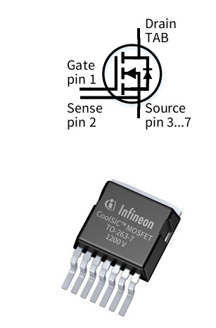
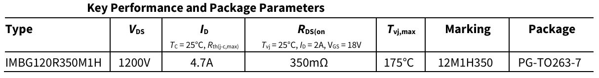
- On Board High Voltage TO263-7 SIC MOSFET (IMBG120R350M1H 1200V/4.7A /350mΩ/175°C)
- Up to 14.0 A typical peak output current (Gate Driver)
- DC-DC Converter Isolation 6.4VKVDC
- Gate Driver Chip Isolation 5.7 kV (rms)
- 3 V and 5 V input supply voltage
- High common-mode transient immunity CMTI > 200 kV/µs
- Screw Terminal Provided for SiC MOSFET Drain Source Connections
- On Board Power LED (Output DC-DC Converter)
- PCB Dimensions 64.93 x 27.31 mm
The module is configured for SiC MOSFET but can also drive MOSFETs and IGBT by replacing the DC-DC converter with the following options:
- R12P22005D: +20/-5V for SiC MOSFETs
- R12P21503D: +15/-3V for SiC MOSFETs
- R12P21509D: +15/-9V for IGBTs
When replacing the DC-DC converter, it’s essential to adjust the gate resistor values (R6 and R9) according to the gate capacitance and response time of the device being driven.
In case of low current output requirement pin to pin compatible chips are available from Infineon
Board Can accommodate Lower Current Chips, few compatible chips list
- 1ED3120MC12H 5.5 A separate source and sink 8.0 V VDE + UL 3120MC12
- 1ED3121MC12H 5.5 A separate source and sink 10.5 V VDE + UL 3121MC12
- 1ED3123MC12H 14.0 A separate source and sink 8.0 V VDE + UL 3123MC12
- 1ED3124MC12H 14.0 A separate source and sink 10.5 V VDE + UL 3124MC12
- 1ED3131MC12H 5.5 A separate source and sink, 180 ns minimum input pulse suppression time
The 1ED3124MC12H gate driver ICs are galvanically isolated single channel gate driver ICs for IGBT, MOSFET and SiC MOSFET in PG-DSO-8 package. They provide a typical output current of up to 14.0 A on separate source and sink pins. The input logic pins operate on a wide input voltage range from 3 V to 15 V using CMOS threshold levels to support 3.3 V microcontrollers. Data transfer across the isolation barrier is realized by the coreless transformer technology. All variants have logic input and driver output undervoltage lockout (UVLO), and active shutdown.
Gate Driver Chip Pin description
- VCC1: Logic input supply voltage of 3.3 V up to 15 V wide operating range
- GND1: Ground connection of input circuit.
- IN+: non-inverted control signal for driver output. An internal filter provides robustness against noise at IN+. An internal weak pull-down resistor favors off-state.
- IN-: Inverted control signal for driver output. An internal filter provides robustness against noise at IN-. An internal weak pull-up resistor favors off-state.
- VCC2: Positive power supply pin of output driving circuit. A proper blocking capacitor has to be placed close to this supply pin.
- VEE2: Reference ground of the output driving circuit. In case of a bipolar supply (positive and negative voltage referred to IGBT emitter) this pin is connected to the negative supply voltage.
- OUT+: Driver source output pin to turn on external IGBT. During on-state the driving output is switched to
- Switching of this output is controlled by IN+ and IN-. This output will also be turned off at an UVLO event.
- OUT-: Driver sink output pin to turn off external IGBT. During off-state the driving output is switched to VEE2.Switching of this output is controlled by IN+ and IN-. In case of UVLO an active shut down keeps the output voltage at a low level.
- OUT: Combined source and sink output pin to external IGBT. The output voltage will be switched between
- VCC2 and VEE2. Switching of this output is controlled by IN+ and IN-. In case of an UVLO event this output will be switched off and an active shut down keeps the output voltage at a low level.
SiC MOSFET Data
Connections
- CN1: Pin 1 = VCC 12V DC Input, Pin 2 = IN+ PWM Input, Pin 3 = IN- PWM Input, Pin 4 = GND-Input Side
- CN2: Pin 1 = Optional Capacitor, Pin 2 = SiC MOSFET Drain, SiC MOSFET Source
- D1: Power LED Output side
Schematic
Parts List
| NO. | QNTY. | REF. | DESC. | MANUFACTURER | SUPPLIER | SUPPLIER PART NO |
|---|---|---|---|---|---|---|
| 1 | 1 | CN1 | 4 PIN MALE HEADER PITCH 2.54MM | WURTH | DIGIKEY | 732-5317-ND |
| 2 | 1 | CN2 | 3 PIN SCREW TERMINAL 7.62MM | WURTH | DIGIKEY | 732-691218410003-ND |
| 3 | 2 | C1,C3 | 1uF/35V CERAMIC SMD SIZE 0805 | YAGEO/MURATA | DIGIKEY | |
| 4 | 1 | C2 | 47uF/25V CERAMIC SMD SIZE 1210 | YAGEO/MURATA | DIGIKEY | |
| 5 | 1 | C4 | 100nF/50V CERAMIC SMD SIZE 0805 | YAGEO/MURATA | DIGIKEY | |
| 6 | 1 | C5 | 10uF/25V CERAMIC SMD SIZE 0805 | YAGEO/MURATA | DIGIKEY | |
| 7 | 2 | C6,C8 | 4.7uF/35V CERAMIC SMD SIZE 0805 | YAGEO/MURATA | DIGIKEY | |
| 8 | 1 | C7 | 1KPF/50V CERMAIC SMD SIZE 0805 | YAGEO/MURATA | DIGIKEY | |
| 9 | 5 | C9,R10,C10,C11,C12 | DNP | |||
| 10 | 1 | D1 | LED RED SMD SIZE 0805 | OSRAM | DIGIKEY | 475-1278-1-ND |
| 11 | 1 | Q1 | IMBG120R350M1H | INFINEON | DIGIKEY | IMBG120R350M1HXTMA1 |
| 12 | 1 | R1 | 4.7K 5% SMD SIZE 0805 | YAGEO/MURATA | DIGIKEY | |
| 13 | 2 | R2,R3 | 12K 5% SMD SZIE 0805 | YAGEO/MURATA | DIGIKEY | |
| 14 | 4 | R4,R5,R7,R8 | 0E SMD SIZE 0805 | YAGEO/MURATA | DIGIKEY | |
| 15 | 2 | R6,R9 | 3.6E 1% SMD SIZE 1206 | YAGEO/MURATA | DIGIKEY | |
| 16 | 1 | U1 | R12P22005D | RCOM | DIGIKEY | 945-3056-ND |
| 17 | 1 | U2 | 1ED3124MC12H | INFINEON | DIGIKEY | 448-1ED3124MC12HXUMA1CT-ND |
Connections
share schematic file
Here is the schematic diagram in PDF: https://www.electronics-lab.com/wp-content/uploads/2025/09/Schematic-1.pdf