Intelligent High-Side Switch with Current Monitor
This high-side switch handles loads up to 10A. It uses an LTC6102 and LT1910 to monitor current and disable the MOSFET upon a fault, with automatic restart.
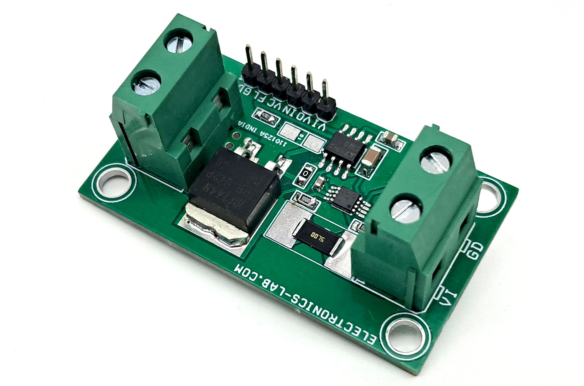
This is an intelligent high-side switch with integrated current monitoring allows users to control loads up to 10A. Upon receiving a trigger signal, the switch activates the load. In the event of a short circuit or overcurrent condition, the output MOSFET is disabled. The system attempts to re-enable the output after a 150ms delay. If the fault persists, this cycle repeats until the fault is cleared. Circuit also provides fault output low Pin5 CN4.
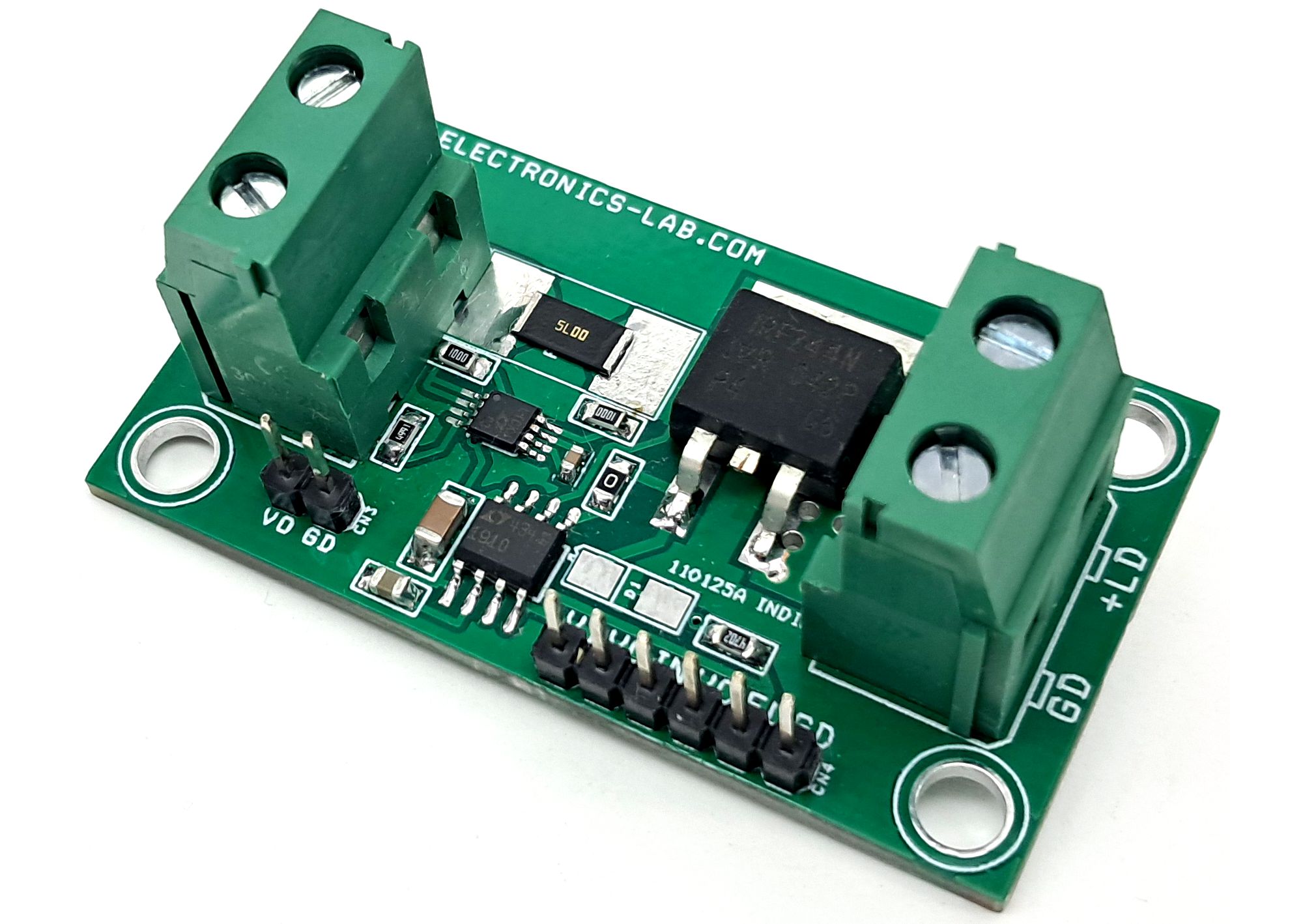
The project consists of LTC6102 precision zero drift current sensor amplifier and LT1910 protected high side MOSFET driver and high current MOSFET SUB85N06-5. The LTC6102 measure the current across current sense resistor and provides the voltage feedback. With 0.005Ohm resistor the feedback is Vo=2.5V at 10A full-scale current . LT1910 is high side gate driver that allows power MOSFET for high side switching applications. LT1910, contains a completely self-contained charge pump to fully enhance an N-channel MOSFET switch with no external components.
When the internal drain comparator senses that the switch current has exceeded the preset level, the switch is turned off and a fault flag is asserted. The switch remains off for a period of time set by an external timing capacitor and then automatically attempts to restart. If the fault still exists, this cycle repeats until the fault is removed, thus protecting the MOSFET. The fault flag becomes inactive once the switch restarts successfully. Test conducted with IRFZ44 MOSFET.
Programmable Current Limit, Delay Time and Auto restart Period
- Default current limit is 10A, this limit can be adjusted with sense resistor R1, Refer the data sheet of LT1920 for more information.
- Default auto restart time is 150mS. User can change the restart time with capacitor C2, Refer the data sheet of LT1920 for more information.
Features
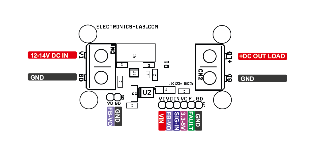
- Input Supply 12-14V DC
- VC 3.3V/5V (This is for Fault Output), Not required If Fault output operation is not used
- Fault Output Low, High = Normal Operations
- Load Current Up to 10Amps
- Load Current Threshold 10Amps
- Automatic MOSFET Off when Short Circuit or Over Current Condition Occurs
- Automatic Restart Time Attempt 150mS
- Precision Current Sense Output 2.5V At full-scale load 10Amps
- High Current Screw Terminals for Input and Output
- The Input Pin Threshold is TTL/CMOS compatible (3.3V-15V)
- 4 x 4MM Mounting Holes
- PCB Dimensions 54.13 x 30.32mm
TIMER (Pin 2): A timing capacitor, CT (C2), from the TIMER pin to ground sets the restart time following overcurrent detection. Upon detection of an overcurrent condition, CT is rapidly discharged to less than 1V and then recharged by a 14µA nominal current source back to the 2.9V timer threshold, whereupon the restart is attempted. Whenever TIMER pulls below 2.9V, the GATE pin pulls low to turn off the external switch. This cycle repeats until the overcurrent condition goes away and the switch restarts successfully. During
CT/C2 = 1µF yields a 150ms restart period.
FAULT (Pin 3): The FAULT pin monitors the TIMER pin voltage and indicates the overcurrent condition. Whenever the TIMER pin is pulled below 3.3V at the onset of a current limit condition, the FAULT pin pulls active LOW. The FAULT pin resets HIGH immediately when the TIMER pin ramps above 3.4V during auto restart. The FAULT pin is an open-collector output, thus requiring an external pull-up resistor and is intended for logic interface. The resistor should be selected with a maximum of 1mA pull-up at low status.
IN (Pin 4): The IN-pin threshold is TTL/CMOS compatible and has approximately 200mV of hysteresis. When the IN pin is pulled active HIGH above 2V, an internal charge pump is activated to pull up the GATE pin. The IN pin can be pulled as high as 15V regardless of whether the supply is on or off. If the IN pin is left open, an internal 75k pull-down resistor pulls the pin below 0.8V to ensure that the GATE pin is inactive LOW.
Input/Supply Sequencing There are no input/supply sequencing requirements for the LT1910. The IN pin may be taken up to 15V with the supply at 0V. When the supply is turned on with the IN-pin set HIGH, the MOSFET turn-on will be inhibited until the timing capacitor charges up to 2.9V (i.e., for one restart cycle).
GATE (Pin 5): The GATE pin drives the power MOSFET gate. When the IN pin is greater than 2V, the GATE pin is pumped approximately 12V above the supply. It has relatively high impedance (the equivalence of a few hundred kΩ) when pumped above the rail. Care should be taken to minimize any loading by parasitic resistance to ground or supply. The GATE pin pulls LOW when the TIMER pin falls below 2.9V.
SENSE (Pin 6): The SENSE pin connects to the input of a supply-referenced comparator with a 65mV nominal offset. When the SENSE pin is taken more than 65mV below supply, the MOSFET gate is driven LOW and the timing capacitor is discharged. The SENSE pin threshold has a 0.33%/°C temperature coefficient (TC), which closely matches the TC of the drain-sense resistor formed from the copper trace of the PCB.
Current Sense Threshold and Feedback Output
The selection of RS should be based on the minimum threshold voltage: RS = 50mV/ISET Thus the 0.005Ω drain-sense resistor in will yield a minimum trip current of 10A. This simple configuration is appropriate for resistive or inductive loads that do not generate large current transients at turn-on. Current feedback Vo=2.5V at 10A full-scale.
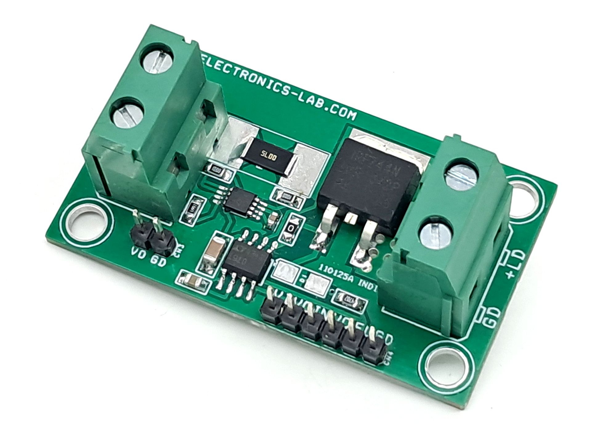
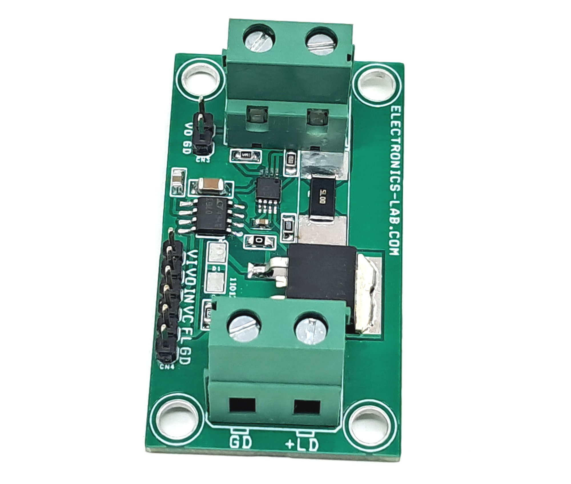
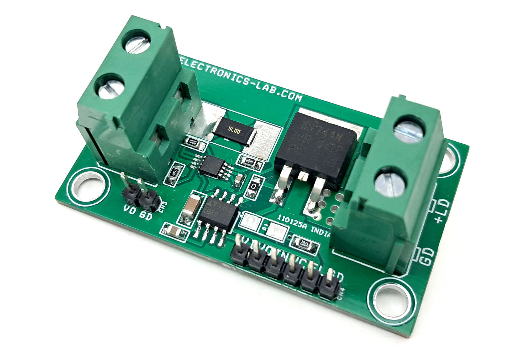
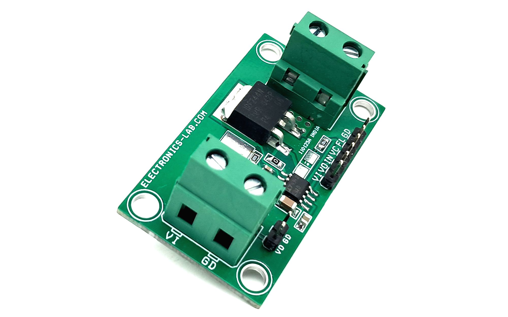
Connections
- CN1: Pin 1 = VI/Power Input 12-14V DC, Pin 2 = GND
- CN2: Pin 1 = +Load, Pin 2 = -Load/GND
- CN3: Pin 1 = VO/Current Feed Back Voltage Output, Pin 2 = GND
- CN4: Pin 1 = VI, Pin 2 = VO, Pin 3 = Trigger Input, Pin 4 = VCC/5V, Pin 5 = Fault, Pin 6 = GND
Schematic
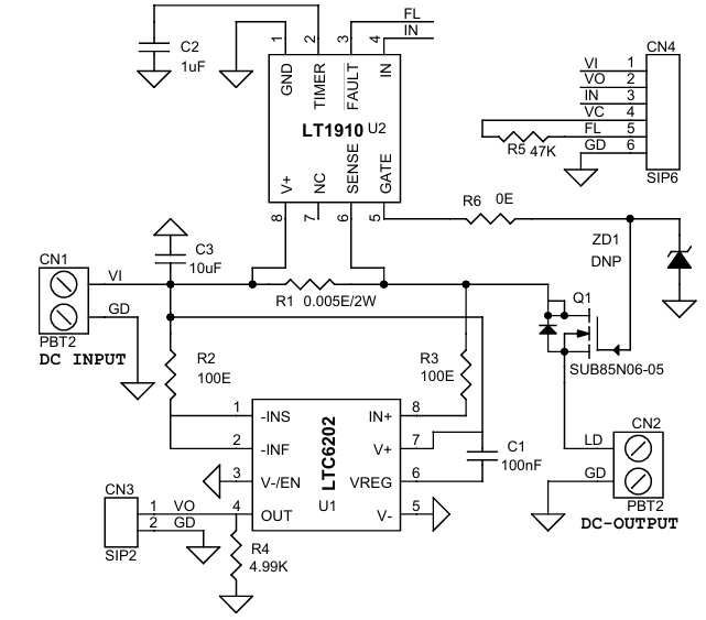
Parts List
| NO. | QNTY. | REF. | DESC. | MANUFACTURER | SUPPLIER | SUPPLIER PART NO |
|---|---|---|---|---|---|---|
| 1 | 2 | CN1,CN2 | 2 PIN SCREW TERMINAL PITCH 7.62MM | AMPHENOL | 609-3954-ND | |
| 2 | 1 | CN3 | 2 MALE HEADER PITCH 2.54MM | WURTH | 732-5315-ND | |
| 3 | 1 | CN4 | 6 PIN MALE HEADER PITCH 2.54MM | WURTH | 732-5319-ND | |
| 4 | 1 | C1 | 100nF/50V CERAMIC SMD SIZE 0603 | YAGEO/MURATA | ||
| 5 | 1 | C2 | 1uF/50V SMD SIZE 0805 | YAGEO/MURATA | ||
| 6 | 1 | C3 | 10uF/50V SMD SIZE 0805 | YAGEO/MURATA | ||
| 7 | 1 | Q1 | SUB85N06-05/STB80NF55-06T4 | ST | 497-6558-1-ND | |
| 8 | 1 | R1 | 0.005E/2W 1% SMD SIZE 2512 | BOURNS INC | CRF2512-FZ-R005ELFCT-ND | |
| 9 | 2 | R2,R3 | 100E 5% SMD SIZE 0805 | YAGEO/MURATA | ||
| 10 | 1 | R4 | 4.99K 1% SMD SIZE 0805 | YAGEO/MURATA | ||
| 11 | 1 | R5 | 47K 5% SMD SIZE 0805 | YAGEO/MURATA | ||
| 12 | 1 | R6 | 0E SMD SIZE 0805 | YAGEO/MURATA | ||
| 13 | 1 | U1 | LTC6102 8MSOP | ANALOG DEVICE | LTC6102IMS8#TRPBFCT-ND | |
| 14 | 1 | U2 | LT1910 SOIC8 | ANALOG DEVICE | LT1910ES8#PBF-ND | |
| 15 | 1 | ZD1 | DNP/OPTIONAL 15V ZENER |
Connections
Block Diagram
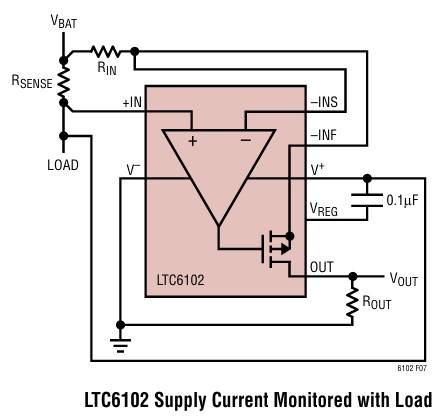
Image courtesy of Analog Devices
Application Diagram
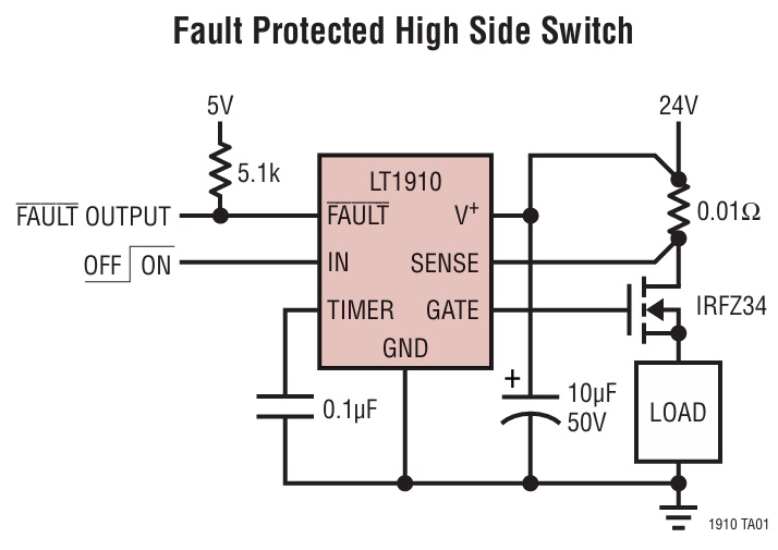
Image courtesy of Analog Devices

Image courtesy of Analog Devices
Timing Diagram
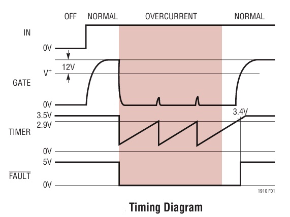
Image courtesy of Analog Devices
Gerber View
Photos