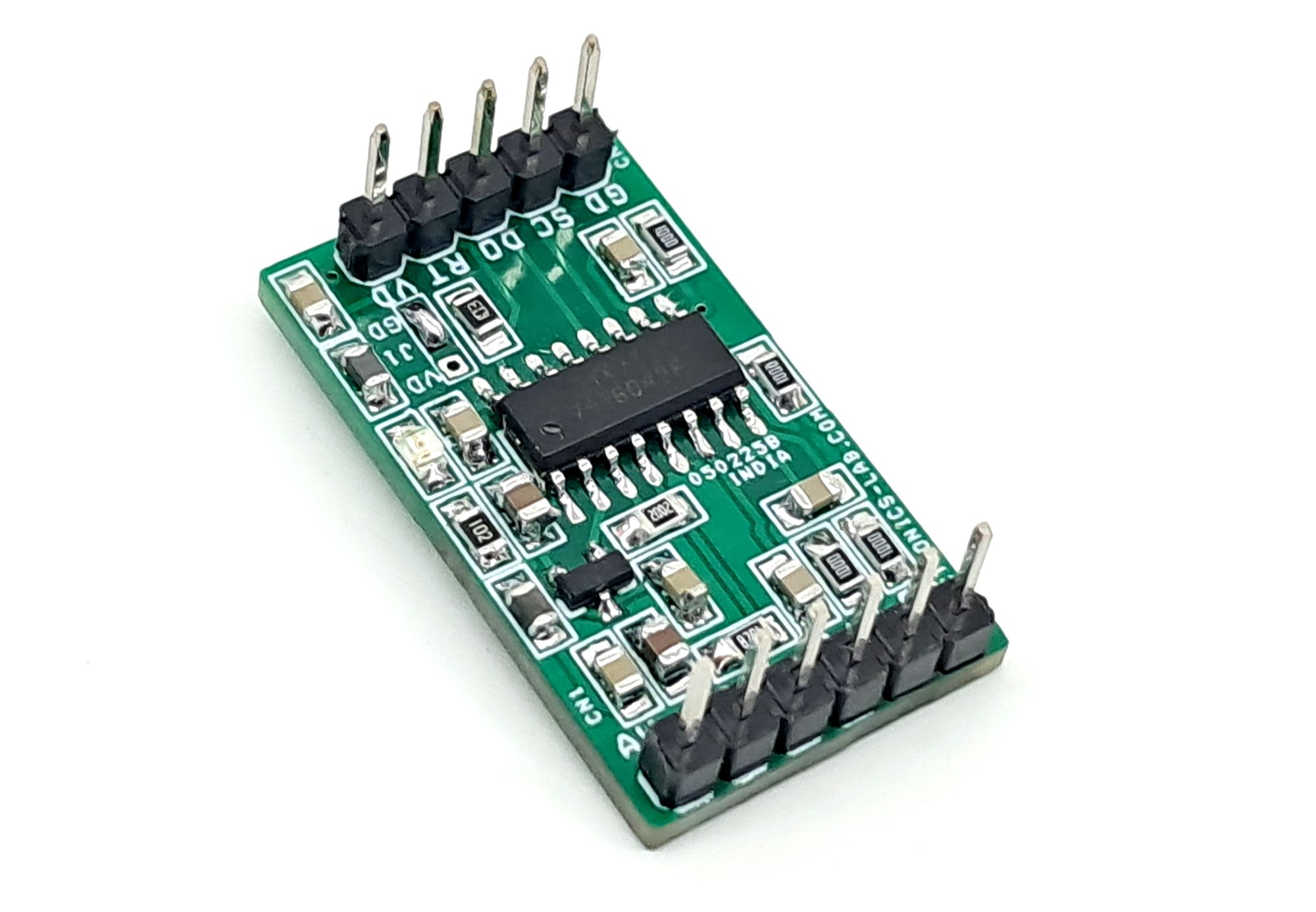
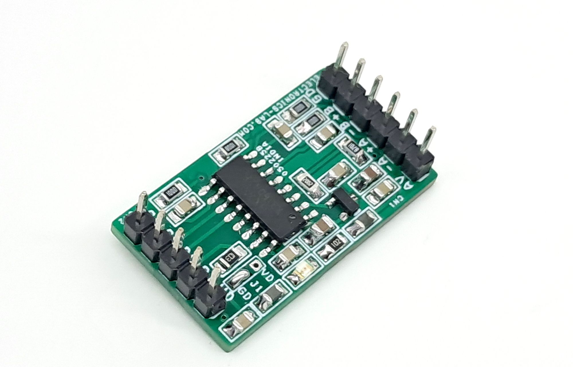
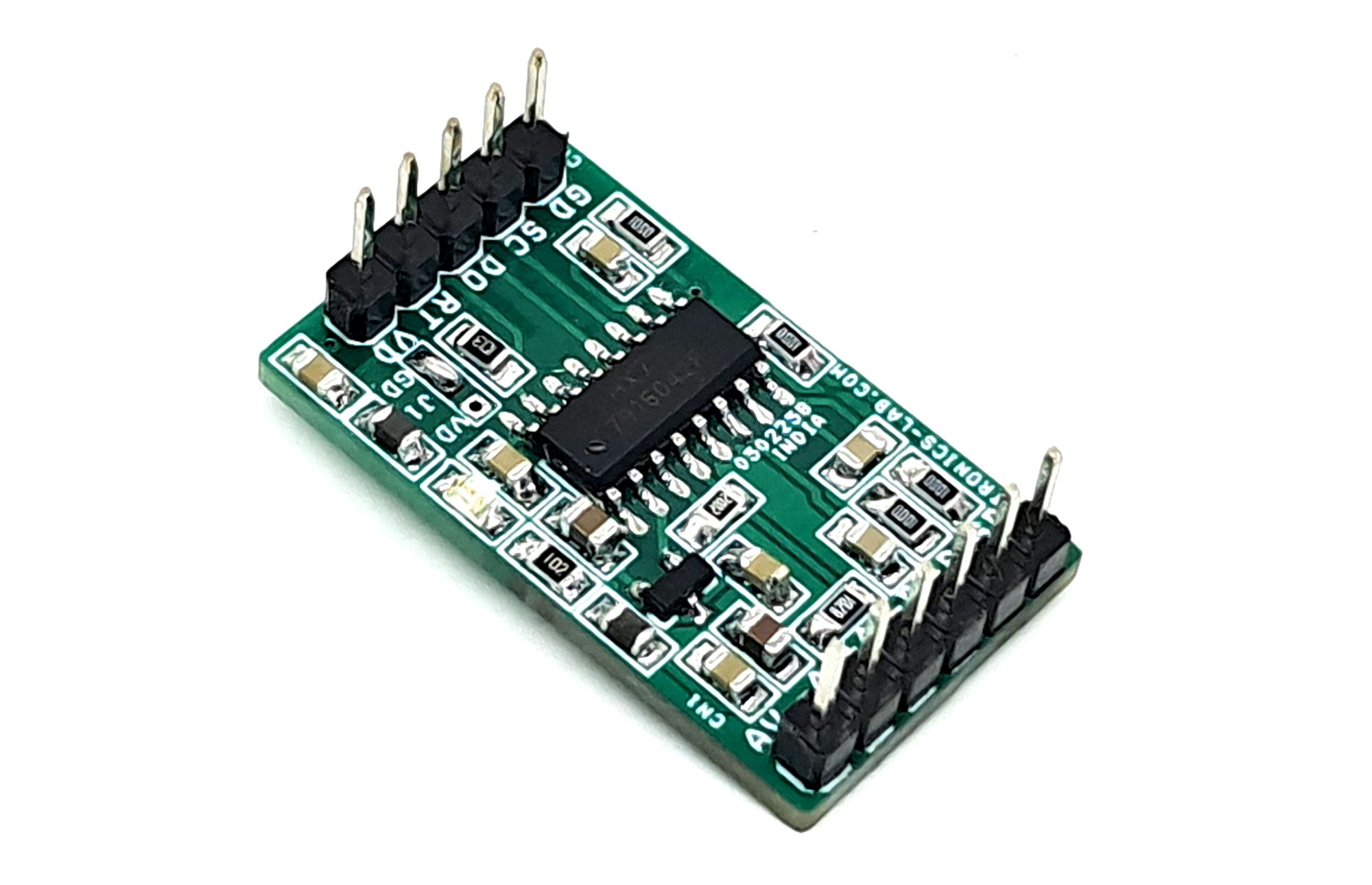
Load Cell Amplifier HX711 for Weigh Scale and Strain Gauge Sensor
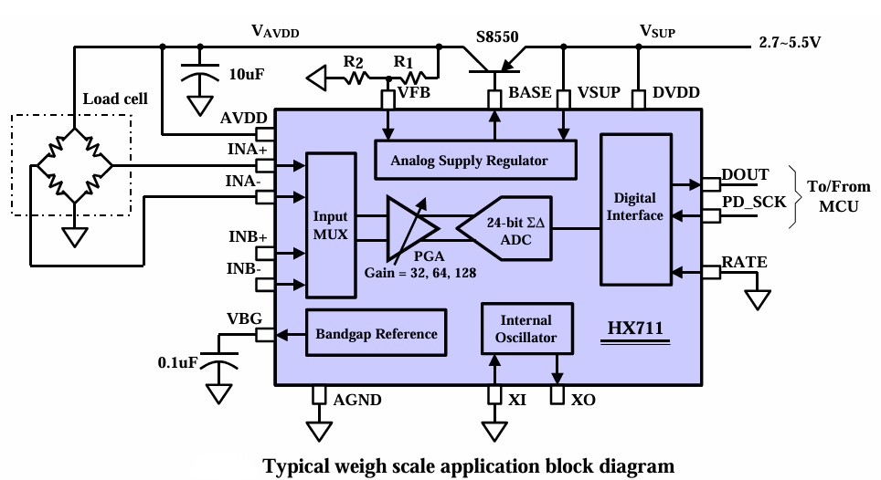
This load cell amplifier uses the HX711 24-bit ADC for weigh scales and control. It directly interfaces with bridge sensors using a PGA (gains of 32, 64, or 128) and includes an on-chip regulator/oscillator, simplifying its use.
This load cell amplifier enables users to measure data from load cells and strain gauges. This project utilizes the HX711 chip, a precision 24-bit analog-to-digital converter (ADC) specifically designed for weigh scales and industrial control applications. The HX711 provides a direct interface with bridge sensors. The input multiplexer selects either Channel A or B differential input to the low-noise programmable gain amplifier (PGA). Channel A can be programmed with a gain of 128 or 64, corresponding to a full-scale differential input voltage of ±20mV or ±40mV respectively, when a 5V supply is connected to AVDD analog power supply pin. Channel B has a fixed gain of 32. On chip power supply regulator eliminates the need for an external supply regulator to provide analog power for the ADC and the sensor. Also there is an on-chip oscillator and does not require any external component. On-chip power on-reset circuitry simplifies digital interface initialization. There is no programming needed for the internal registers. All controls to the HX711 are through the header connector. Jumper J1 connect it to GND for normal Operation.
Features
- Operation supply voltage range: 2.6 ~ 5.5V
- On-chip active low noise PGA with selectable gain of 32, 64 and 128
- On Board Power LED
- Header Connectors for Inputs (Sensor) , Output, Data and Power Input
- On-chip power supply regulator for load-cell and
- ADC analog power supply
- On-chip oscillator requiring no external component with optional external crystal
- On-chip power-on-reset
- Simple digital control and serial interface: pin-driven controls, no programming needed
- Selectable 10SPS or 80SPS output data rate
- Simultaneous 50 and 60Hz supply rejection
- Two selectable differential input channels
- Current consumption including on-chip analog power supply regulator: normal operation < 1.5mA, power down < 1uA
- PCB Dimensions 30.00 x 17.30 mm
Analog Inputs
Channel A differential input is designed to interface directly with a bridge sensor’s differential output. It can be programmed with a gain of 128 or 64. The large gains are needed to accommodate the small output signal from the sensor. When 5V supply is used at the AVDD pin, these gains correspond to a full-scale differential input voltage of ±20mV or ±40mV respectively. Channel B differential input has a fixed gain of 32. The full-scale input voltage range is ±80mV, when 5V supply is used at the AVDD pin.
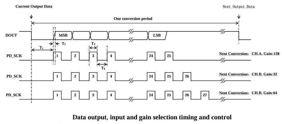
Output Data Rate and Format
When using the on-chip oscillator, output data rate is typically 10 (RATE=0) or 80SPS (RATE=1). When using external clock or crystal, output data rate is directly proportional to the clock or crystal frequency. Using 11.0592MHz clock or crystal results in an accurate 10 (RTE=0) or 80SPS (RATE=1) output data rate. The output 24 bits of data is in 2’s complement format. When input differential signal goes out of the 24-bit range, the output data will be saturated at 800000h (MIN) or 7FFFFFh (MAX), until the input signal comes back to the input range.
Power Supply Options
Digital power supply (DVDD) should be the same power supply as the MCU power supply. When using internal analog supply regulator, the dropout voltage of the regulator depends on the external transistor used. The output voltage is equal to VAVDD=VBG*(R1+R2)/ R1 (Fig. 1). This voltage should be designed with a minimum of 100mV below VSUP voltage.
Serial Interface
Pin PD_SCK and DOUT are used for data retrieval, input selection, gain selection and power down controls. When output data is not ready for retrieval, digital output pin DOUT is high. Serial clock input PD_SCK should be low. When DOUT goes to low, it indicates data is ready for retrieval. By applying 25~27 positive clock pulses at the PD_SCK pin, data is shifted out from the DOUT output pin. Each PD_SCK pulse shifts out one bit, starting with the MSB bit first, until all 24 bits are shifted out. The 25th pulse at PD_SCK input will pull DOUT pin back to high.
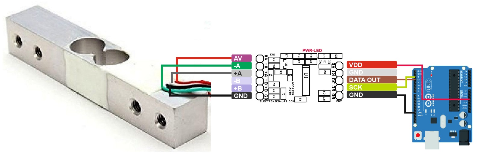
Arduino Code
Arduino Code available for testing purpose, D2 and D3 pin used for Arduino interface. User will able to read the sensor value on serial print.
/*
 Example using the SparkFun HX711 breakout board with a scale
 By: Nathan Seidle
 SparkFun Electronics
 Date: November 19th, 2014
 License: This code is public domain but you buy me a beer if you use this and we meet someday (Beerware license).

 This example demonstrates basic scale output. See the calibration sketch to get the calibration_factor for your
 specific load cell setup.

 This example code uses bogde's excellent library:"https://github.com/bogde/HX711"
 bogde's library is released under a GNU GENERAL PUBLIC LICENSE

 The HX711 does one thing well: read load cells. The breakout board is compatible with any wheat-stone bridge
 based load cell which should allow a user to measure everything from a few grams to tens of tons.
 Arduino pin 2 -> HX711 CLK
 3 -> DAT
 5V -> VCC
 GND -> GND

 The HX711 board can be powered from 2.7V to 5V so the Arduino 5V power should be fine.

*/

#include "HX711.h"

#define calibration_factor -390000.0 //This value is obtained using the SparkFun_HX711_Calibration sketch

#define LOADCELL_DOUT_PIN  3
#define LOADCELL_SCK_PIN  2

HX711 scale;

void setup() {
  Serial.begin(9600);
  Serial.println("HX711 scale demo");

  scale.begin(LOADCELL_DOUT_PIN, LOADCELL_SCK_PIN);
  scale.set_scale(calibration_factor); //This value is obtained by using the SparkFun_HX711_Calibration sketch
  scale.tare(); //Assuming there is no weight on the scale at start up, reset the scale to 0

  Serial.println("Readings:");
}

void loop() {
  Serial.print("Reading: ");
  Serial.print(scale.get_units(), 1); //scale.get_units() returns a float
  Serial.print(" Kg"); //You can change this to kg but you'll need to refactor the calibration_factor
  Serial.println();
}
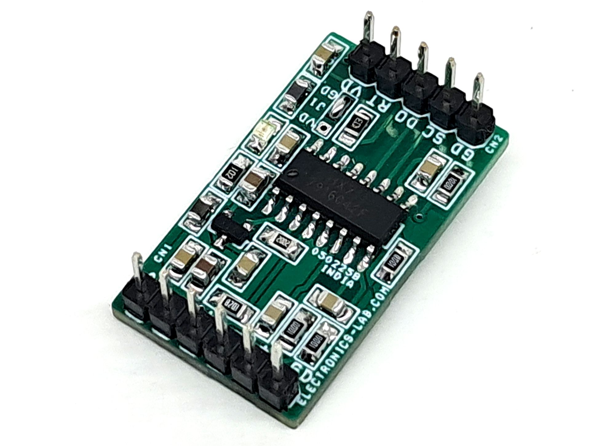
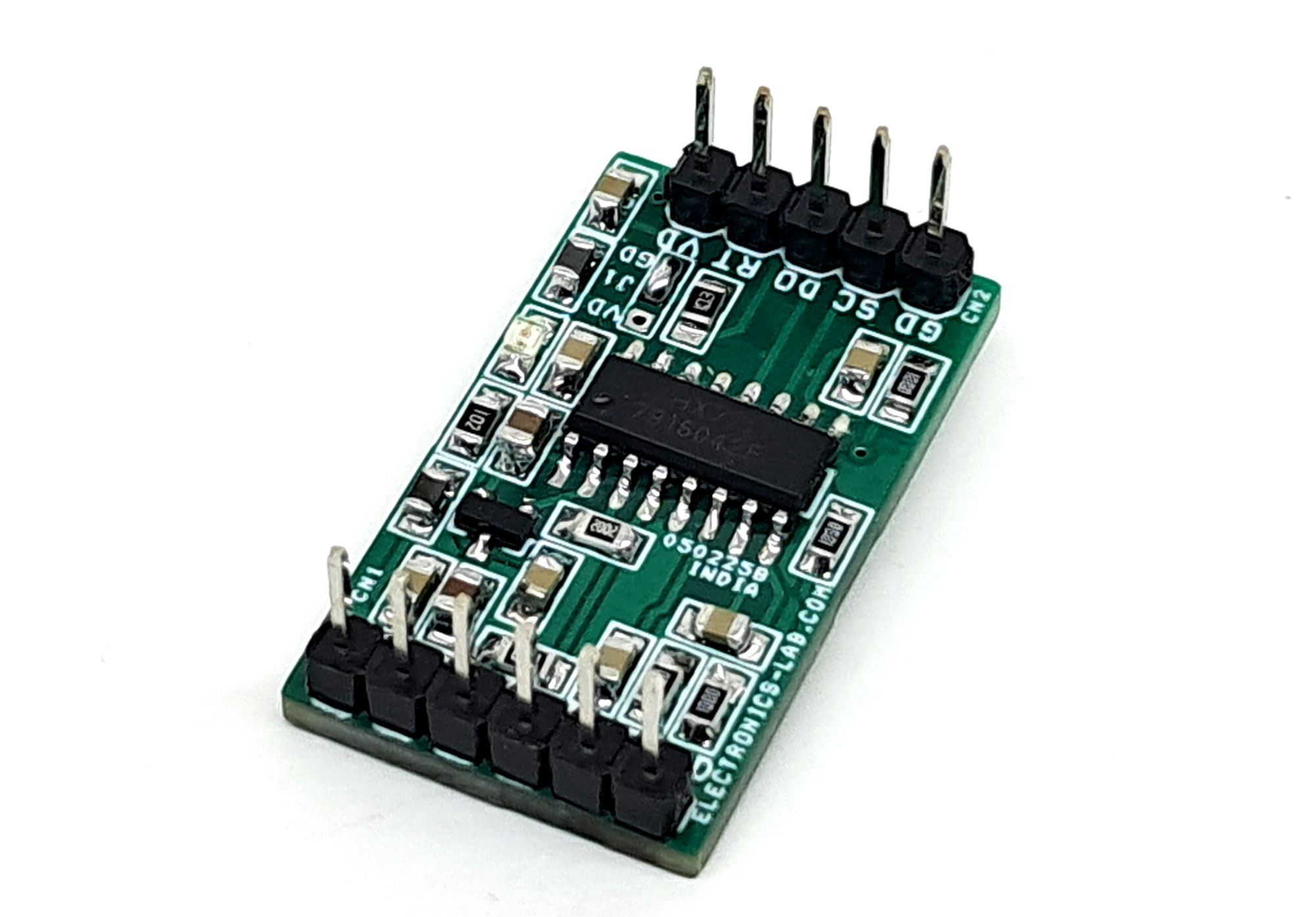
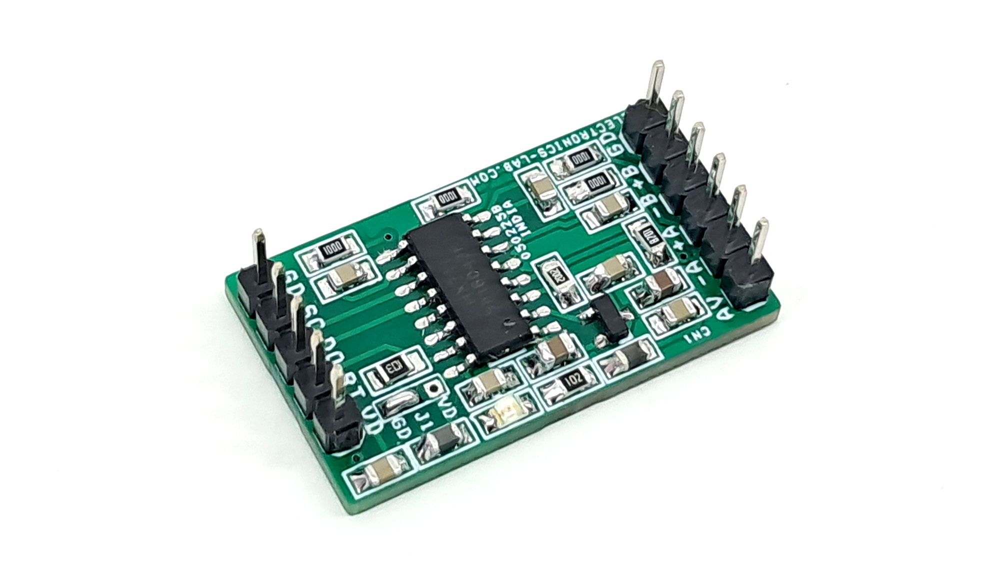
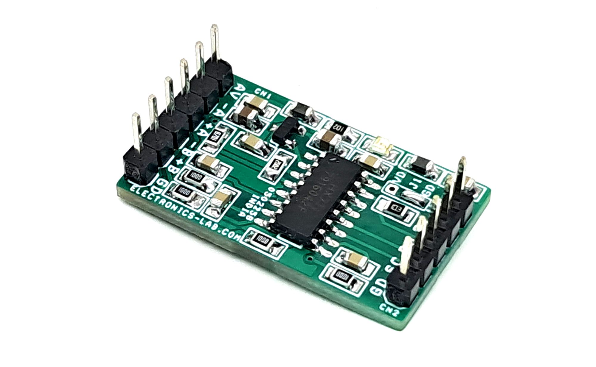
Connections
- CN1 Load Cell Sensor: Pin 1 = AV/+Voltage, Pin 2 = Sensor A-, Pin 3 = Sensor A+, Pin 4 = Sensor B-, Pin 5 = Sensor B+, Pin 6 = GND
- CN2: Pin 1 = VDD/5V DC Input, Pin 2 = RT, Pin 3 = Data Output, Pin 4 = SCL, Pin 5 = GND
- D1: Power LED
Schematic
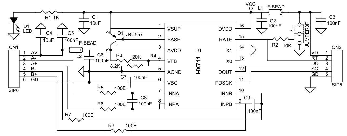
Parts List
| N0. | QNTY. | REF. | DESC. | MANUFACTURER | SUPPLIER | SUPPLIER PART NO |
|---|---|---|---|---|---|---|
| 1 | 1 | CN1 | 6 PIN MALE HEADER PITCH 2.54MM | WURTH | DIGIKEY | 732-5319-ND |
| 2 | 1 | CN2 | 5 PIN MALE HEADER PITCH 2.54MM | WURTH | DIGIKEY | 732-5318-ND |
| 3 | 2 | C1,C4 | 10uF/16V CERAMIC SMD SIZE 0805 | YAGEO/MURATA | DIGIKEY | |
| 4 | 7 | C2,C3,C5,C6,C7,C8,C9 | 100nF/50V CERAMIC SMD SIZE 0805 | YAGEO/MURATA | DIGIKEY | |
| 5 | 1 | D1 | LED RED SMD SIZE 0805 | OSRAM | DIGIKEY | 475-1278-1-ND |
| 6 | 1 | J1 | JUMPER3P | PCB SOLDER JUMPER | ||
| 7 | 2 | L1,L2 | FERRITE-BEAD 600-OHM SMD SIZE 0805 | LAIRD | DIGIKEY | 240-2390-1-ND |
| 8 | 1 | Q1 | S8550 BJT-PNP SMD SOT23-3 | UMW | DIGIKEY | 4518-S8550CT-ND |
| 9 | 1 | R1 | 1K 5% SMD SIZE 0805 | YAGEO/MURATA | DIGIKEY | |
| 10 | 1 | R2 | 10K 5% SMD SIZE 0805 | YAGEO/MURATA | DIGIKEY | |
| 11 | 1 | R3 | 20K 5% SMD SIZE 0805 | YAGEO/MURATA | DIGIKEY | |
| 12 | 1 | R4 | 8.2K 5% SMD SIZE 0805 | YAGEO/MURATA | DIGIKEY | |
| 13 | 4 | R5,R6,R7,R8 | 100E 5% SMD SIZE 0805 | YAGEO/MURATA | DIGIKEY | |
| 14 | 1 | U1 | HX711 | AVIA SEMICON | https://www.lcsc.com/ | C6705483 |
Connections
Application Diagram
Input – Output Waveforms
Gerber View
Photos