Mini Power Monitor Shield for OLEDUINO v2 using INA219
INA219 Monitor Shield: Compact OLEDUINO-v2 add-on. Measures load current, bus voltage, and power via screw terminals.
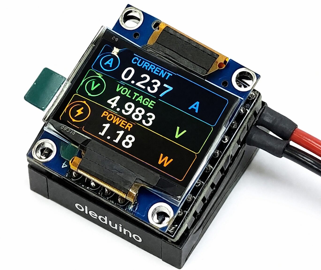
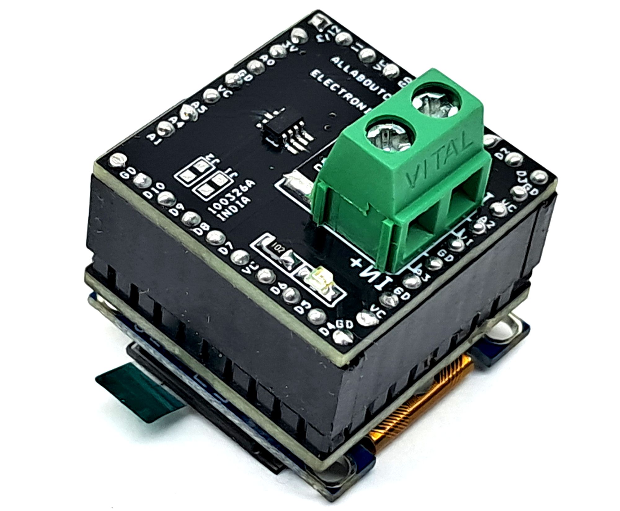
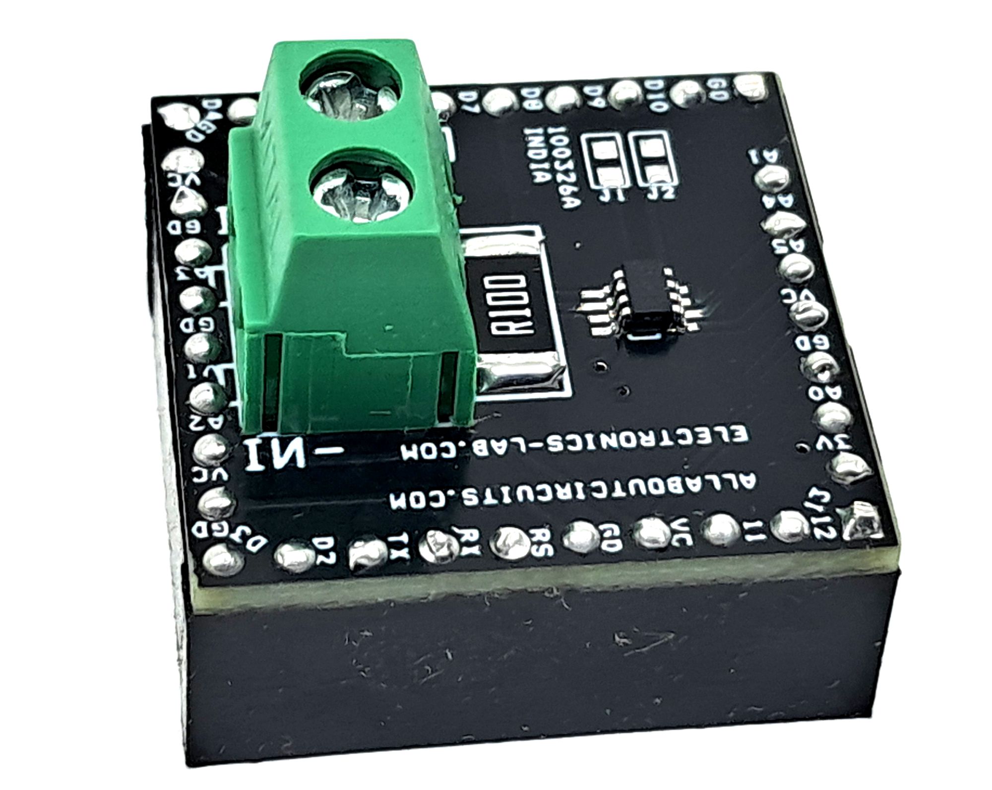
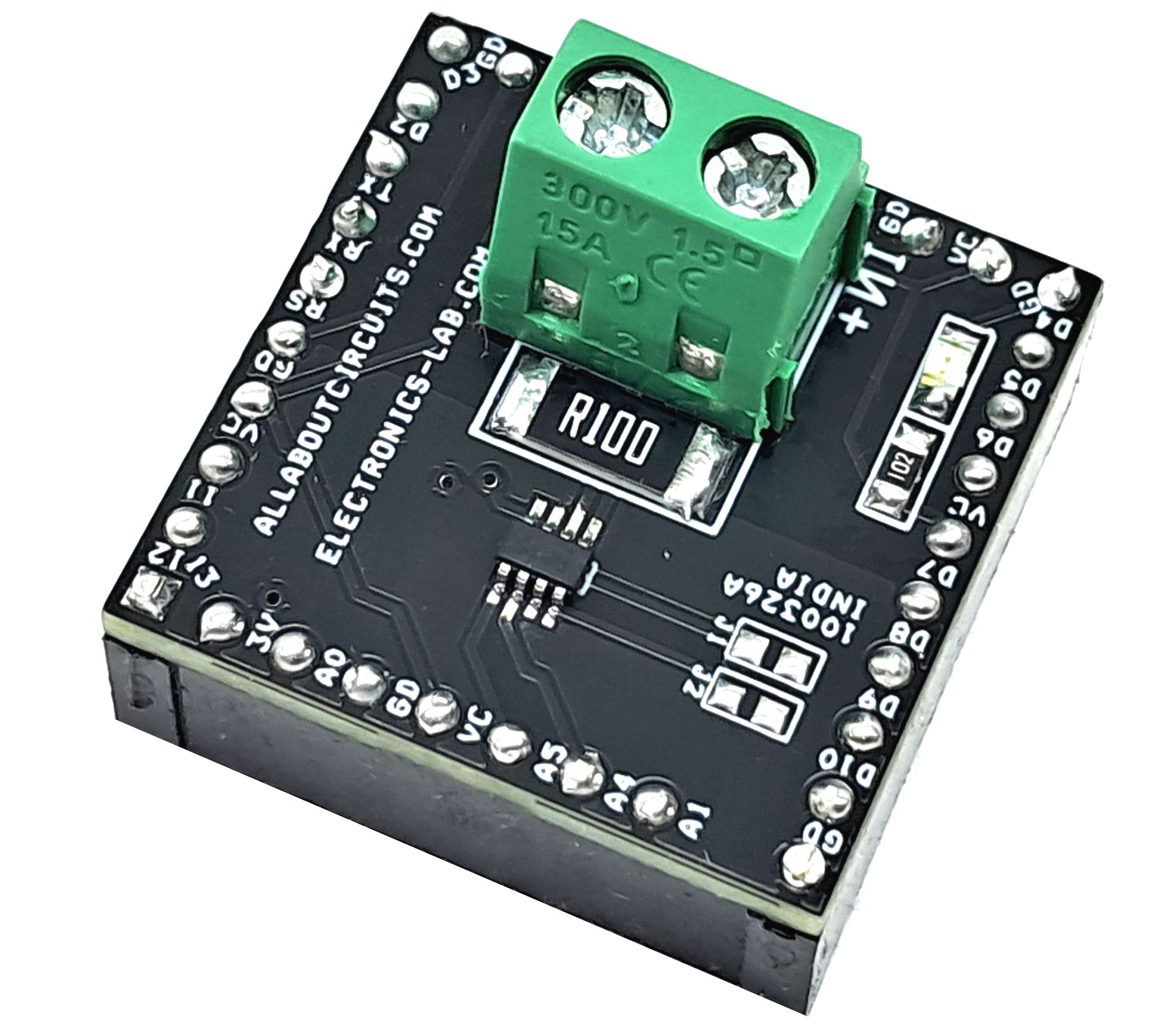
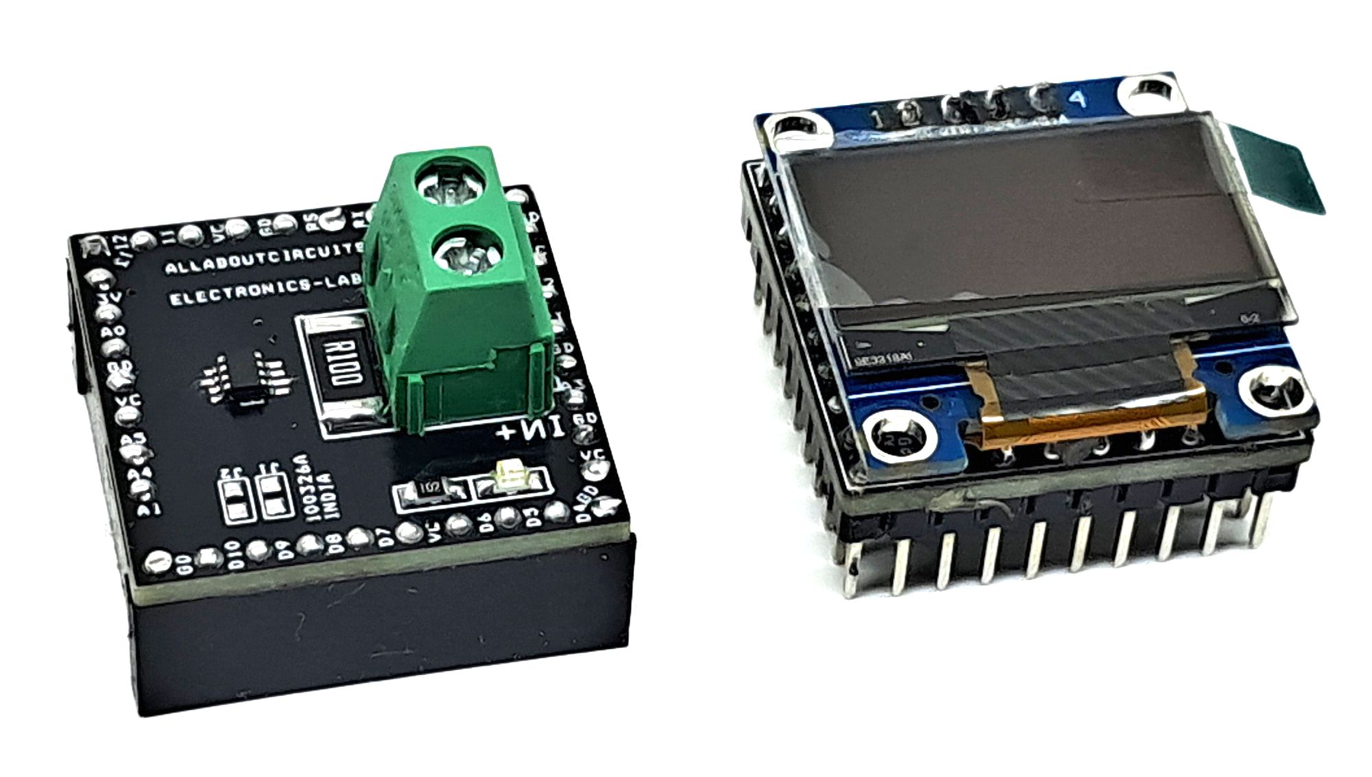
This is a compact bidirectional current and power monitor shield designed for the OLEDUINO-v2. The shield is built around the INA219 chip and includes screw terminals for easy connection of the load, allowing accurate measurement of current, bus voltage, and power.
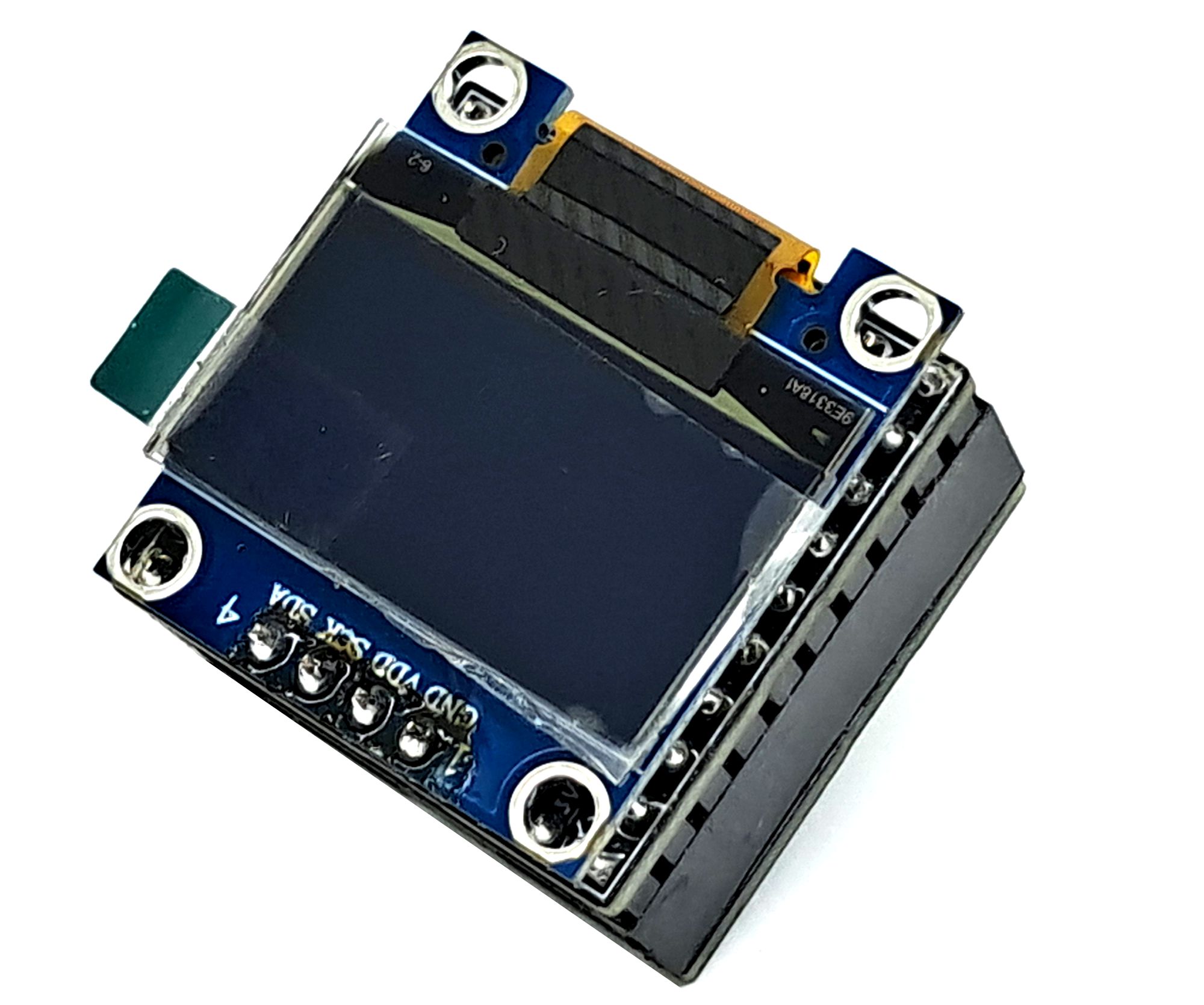
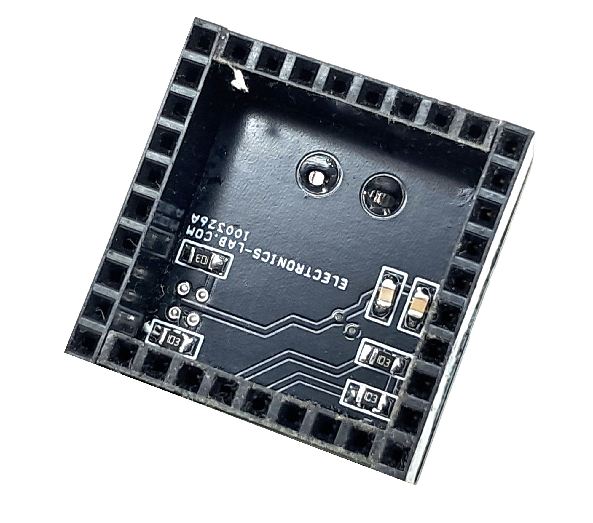
The shield can be mounted on the back side of the OLEDUINO-V2, creating a very compact current and power monitoring solution. The INA219 communicates using the I²C protocol, making integration simple and efficient.
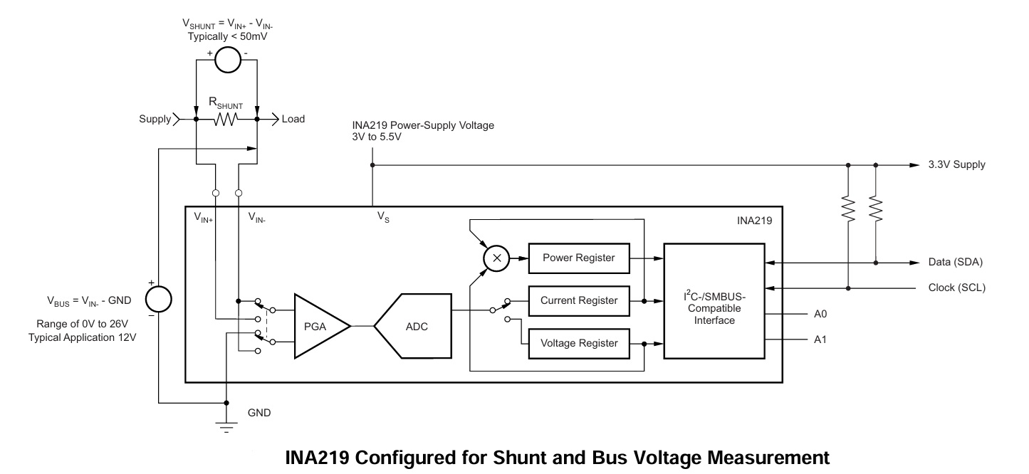
The INA219 is a current shunt and power monitor with an I²C- or SMBus-compatible interface. It measures both the voltage drop across the shunt resistor and the bus supply voltage. The device features programmable conversion times and filtering options for improved measurement accuracy.
A programmable calibration register, combined with an internal multiplier, enables direct current readings in amperes. Additionally, an internal power calculation register provides power readings in watts. The interface supports up to 16 programmable addresses, allowing multiple devices on the same bus.
Arduino Code
Arduino code is provided and intended to test the shield. Upload the code to the OLEDUINO-V2 using the programming connector. Once uploaded, the user will be able to measure current and power.
Compatible with OLEDUINO v2: https://www.electronics-lab.com/project/oleduino-v-2/
Key Features
- Shield Power 5V DC
- Measures bus voltages from 0 to 26 V
- Measures Current +/- 3.2A (0.8mA Resolution)
- Reports current, voltage, and power
- 16 programmable I²C addresses
- High accuracy: up to 0.5% (maximum) over temperature (INA219B)
- Configurable filtering options
- Programmable calibration registers
- On Board Power LED
- PCB Dimensions 25.4 x 25.4 mm
Power Measurement
Current and bus voltage are converted at different points in time, depending on the resolution and averaging mode settings. For instance, when configured for 12-bit and 128 sample averaging, up to 68 ms in time between sampling these two values is possible. Again, these calculations are performed in the background and do not add to the overall conversion time.
PGA Function
If larger full-scale shunt voltages are desired, the INA219 provides a PGA function that increases the full-scale range up to 2, 4, or 8 times (320 mV). Additionally, the bus voltage measurement has two full-scale ranges: 16 or 32 V.
Programming
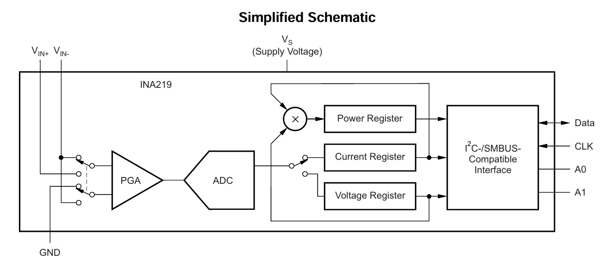
An important aspect of the INA219 device is that it measures current or power if it is programmed based on the system. The device measures both the differential voltage applied between the IN+ and IN- input pins and the voltage at IN- pin. In order for the device to report both current and power values, the user must program the resolution of the Current Register (04h) and the value of the shunt resistor (RSHUNT) present in the application to develop the differential voltage applied between the input pins. Both the Currents and shunt resistor value are used in the calculation of the Calibration Register value that the device uses to calculate the corresponding current and power values based on the measured shunt and bus voltages. After programming the Calibration Register, the Current Register (04h) and Power Register (03h) update accordingly based on the corresponding shunt voltage and bus voltage measurements. Until the Calibration Register is programmed, the Current Register (04h) and Power Register (03h) remain at zero.
The INA219 offers compatibility with both I2C and SMBus interfaces. The I2C and SMBus protocols are essentially compatible with one another. The I2C interface is used throughout this data sheet as the primary example, with SMBus protocol specified only when a difference between the two systems is being addressed. Two bidirectional lines, SCL and SDA, connect the INA219 to the bus. Both SCL and SDA are open-drain connections. The device that initiates the transfer is called a master, and the devices controlled by the master are slaves. The bus must be controlled by a master device that generates the serial clock (SCL), controls the bus access, and generates START and STOP conditions. To address a specific device, the master initiates a START condition by pulling the data signal line (SDA) from a HIGH to a LOW logic level while SCL is HIGH. All slaves on the bus shift in the slave address byte on the rising edge of SCL, with the last bit indicating whether a read or write operation is intended. During the ninth clock pulse, the slave being addressed responds to the master by generating an Acknowledge and pulling SDA LOW. Data transfer is then initiated and eight bits of data are sent, followed by an Acknowledge bit. During data transfer, SDA must remain stable while SCL is HIGH. Any change in SDA while SCL is HIGH is interpreted as a START or STOP condition. Once all data have been transferred, the master generates a STOP condition, indicated by pulling SDA from LOW to HIGH while SCL is HIGH. The INA219 includes a 28-ms timeout on its interface to prevent locking up an SMBus.
The INA219 operates only as a slave device on the I2C bus and SMBus. Connections to the bus are made through the open-drain I/O lines SDA and SCL. The SDA and SCL pins feature integrated spike suppression filters and Schmitt triggers to minimize the effects of input spikes and bus noise. The INA219 supports the transmission protocol for fast (1- to 400-kHz) and high-speed (1-kHz to 2.56-MHz) modes. All data bytes are transmitted most significant byte first.
INA219/OLED Display Pins VS Arduino (OLEDUINO-V2) Pins
- INA219 SDA = Arduino (OLEDUINO-V2) A4
- INA219 SCL = Arduino (OLEDUINO-V2) A5
- OLEDUINO-V2 SDA = Arduino (OLEDUINO-V2) A4
- OLEDUINO-V2 SCL = Arduino (OLEDUINO-V2) A5
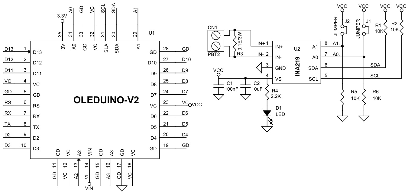
Connections
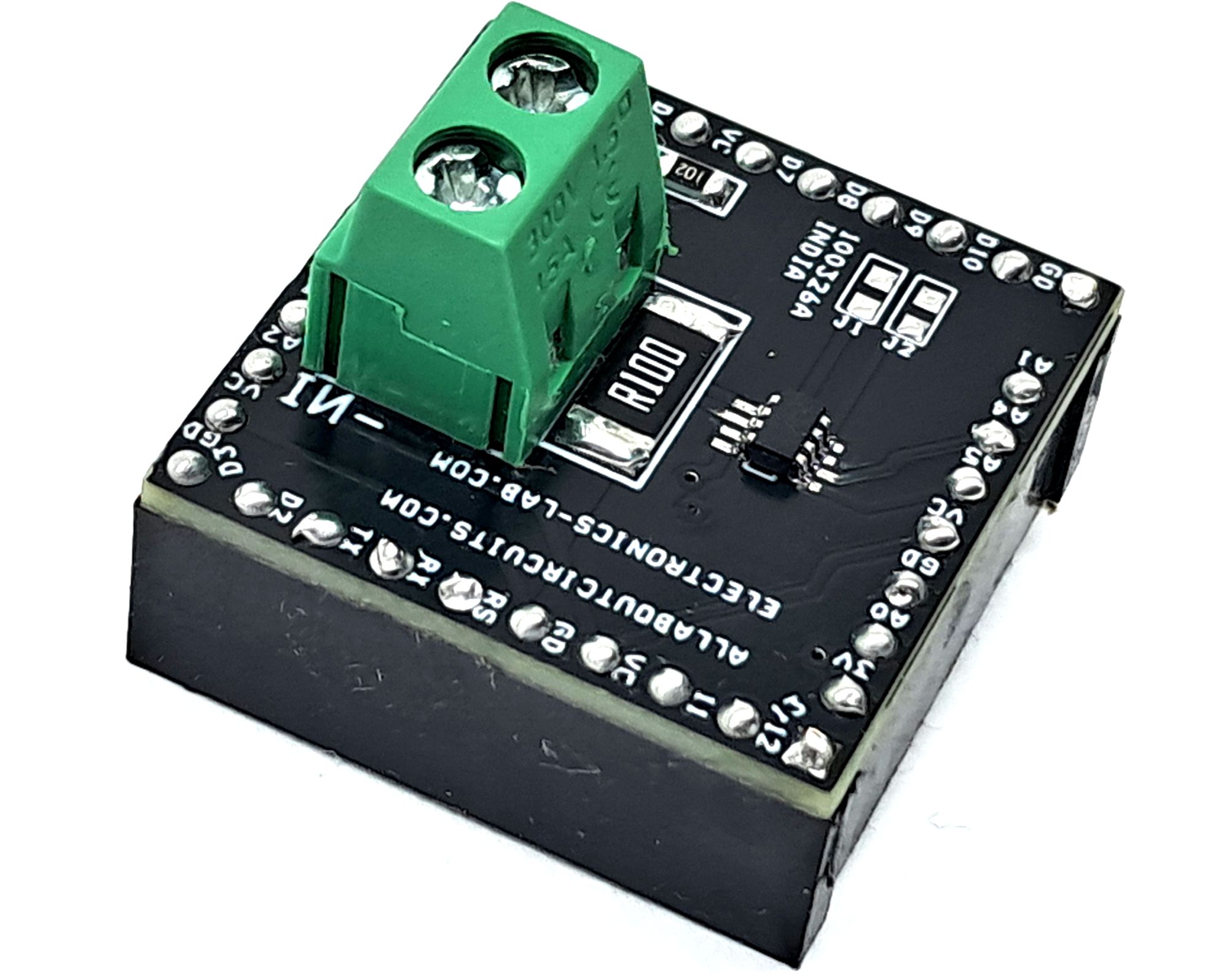
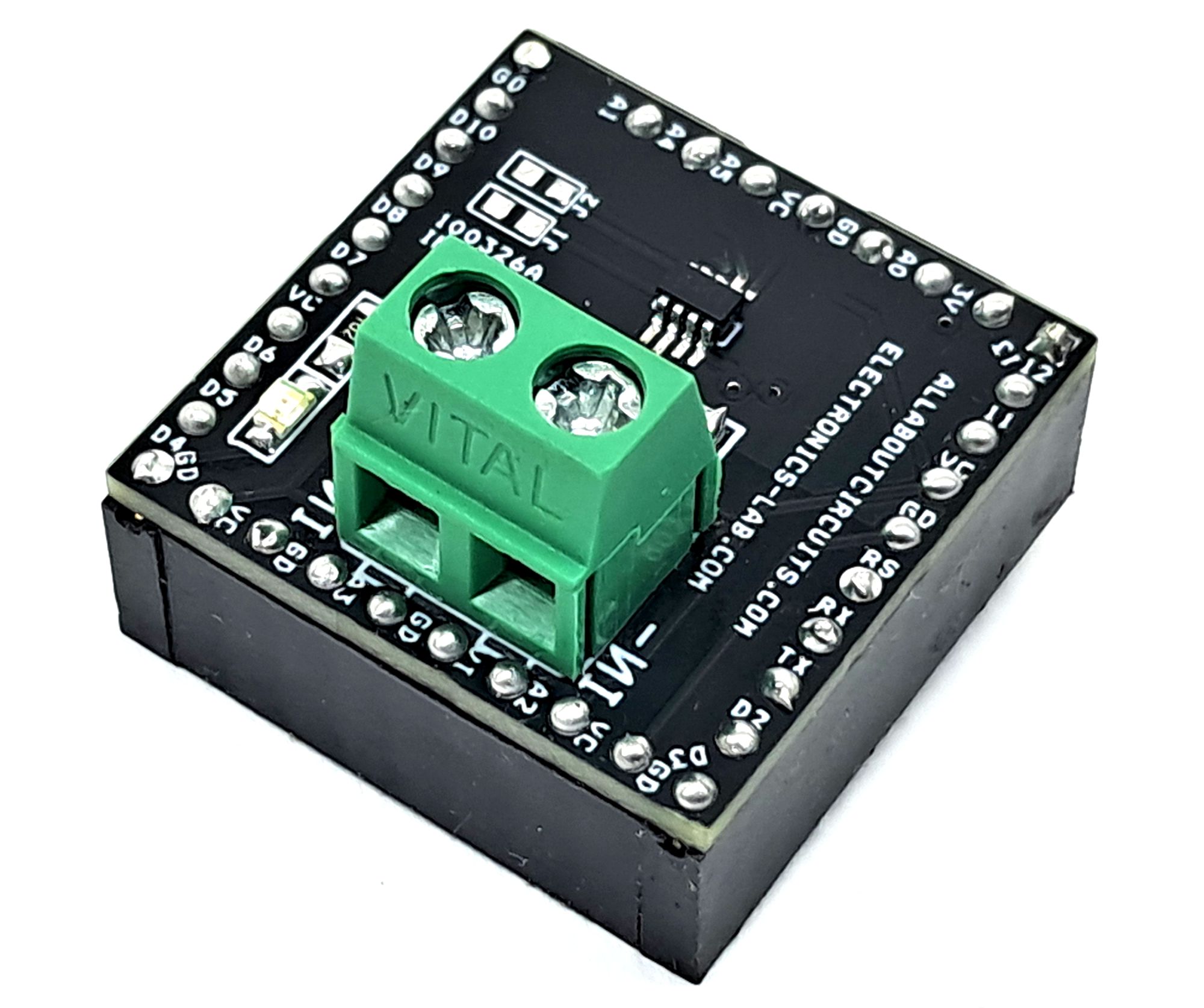
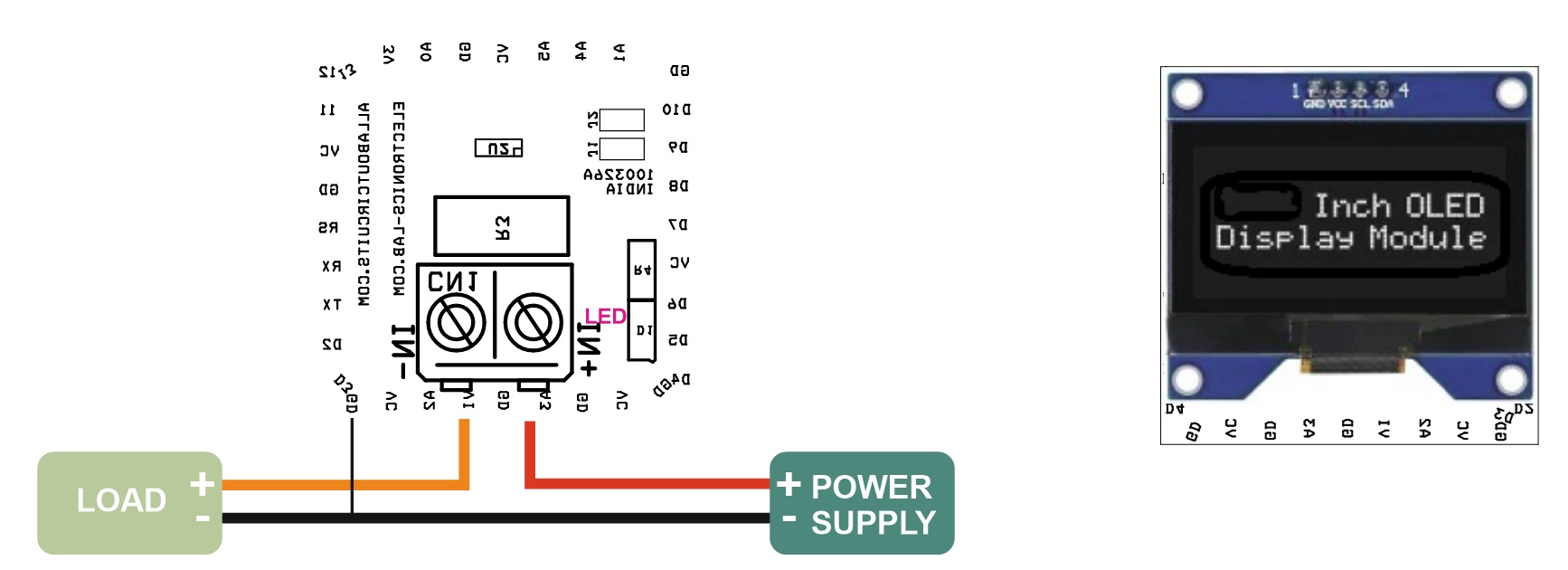
- CN1: Pin 1 = Load IN+, Pin 2 = Load IN-
- Jumper J1: I2C Address
- Jumper J2: I2C Address
- D1: Power LED
Schematic
Parts List
| NO. | QNTY. | REF. | DESC | MANUFACTURER | SUPPLIER | SUPPLIER PART NO |
|---|---|---|---|---|---|---|
| 1 | 1 | CN1 | 2 PIN SCREW TERMINAL PITCH 5.08MM | PHOENIX | DIGIKEY | 277-1247-ND |
| 2 | 1 | C1 | 100nF/50V CERAMIC SMD SIZE 0805 | YAGEO/MURATA | DIGIKEY | |
| 3 | 1 | C2 | 10uF/25V CERAMIC SMD SIZE 0805 | YAGEO/MURATA | DIGIKEY | |
| 4 | 1 | D1 | LED RED SMD SIZE 0805 | OSRAM | DIGIKEY | 475-1278-1-ND |
| 5 | 2 | J1,J2 | JUMPER PCB SOLDER | |||
| 6 | 4 | R1,R2,R5,R6 | 10K 5% SMD SIZE 0805 | YAGEO/MURATA | DIGIKEY | |
| 7 | 1 | R3 | 0.1E/3W 1% SMD SIZE 2512 | BOURNS | DIGIKEY | CRA2512-FZ-R100ELFCT-ND |
| 8 | 1 | R4 | 2.2K 5% SMD SIZE 0805 | YAGEO/MURATA | DIGIKEY | |
| 9 | 1 | U1 | OLEDUINO-V2 | EL | DIGIKEY | |
| 10 | 1 | U2 | INA219 | TI | DIGIKEY | 296-46420-1-ND |
| 11 | 2 | CN2 | 8 PIN MALE HEADER PITCH 2.54MM | WURTH | DIGIKEY | 732-5321-ND |
| 12 | 2 | CN3 | 10 PIN MALE HEADER PITCH 2.54MM | WURTH | DIGIKEY | 732-2670-ND |
Application Diagram
INA219 Block Diagram
Connections
Gerber View
Photos