Overvoltage, Undervoltage and Reverse Supply Protection Controller
This project is a High Voltage Protection Controller using the LTC4365 chip and MOSFETs. It shields the load from undervoltage (5V), overvoltage (18V), and reverse polarity by controlling the MOSFET gates. The LTC4365 withstands −40V to 60V and features a 36ms turn-on delay and a FAULT indicator pin.
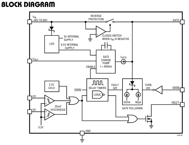
This is a High Voltage Undervoltage (UV), Overvoltage (OV) and Reverse Supply Protection Controller consists of LTC4365 chip and MOSFET. The controller protects the load circuit from input voltages that may be too high, too low or negative. It operates by controlling the gates of two back-back connected MOSFETs to keep the output in safe range. The OV and UV protection levels are adjusted by resistive dividers at the OV and UV pins. Asserting the SHDN pin disables the MOSFETs and places the LTC4365 in a low-current shutdown state. The FAULT pin is asserted when the controller is in shutdown mode or when the input voltage is outside of the UV or OV level. The LTC4365 can withstand DC voltages between -40V and 60V and has a valid operating range 2.4V to 35V. In this project the circuit is optimized for 12V DC, Undervoltage is set to 5V DC and Overvoltage is 18V DC.
The LTC4365 monitors the input rail voltage and disconnects downstream circuits when the input voltage is too low, too high or negative. The LTC4365 provides accurate overvoltage and undervoltage comparators to ensure that power is applied to the system only if the input supply is within the allowable voltage window. Reverse supply protection circuit automatically isolates the load from negative input voltages. During normal operation, a high voltage charge pump enhances the gate of external N-channel power MOSFETs. The LTC4365 consumes 10µA during shutdown and 125µA while operating. The LTC4365 has a 36ms turn-on delay that debounces live connections and blocks 50Hz to 60Hz AC power. For fast recovery after faults.
Features
- Input Operating Voltage 12V (Range 6V to 18V)
- Output 12V DC (Range 6V to 18V)
- Load Current 3Amps (MOSFET8.5A)
- On Board Output LED
- On Board Fault LED
- Screw Terminal for Inputs and Outputs
- Reverse Supply Protection to -40V
- UV Input Threshold Voltage 500mV
- UV Input Hysteresis 25mV
- OV Input Threshold Voltage 500mV
- OV Input Hysteresis 25mV
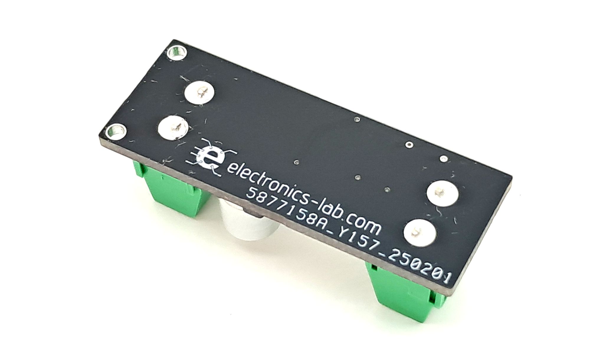
- PCB Dimensions 38.89 x 14.61 mm
Applications
- The battery is installed backwards
- An AC adaptor of opposite polarity is attached
- An AC adaptor of excessive voltage is attached
- The battery is discharged below a safe level
Power LED and Fault LED
- Input Voltage 0 to 5V, Output LED off and Fault LED on (Output Off)
- Input Voltage Above 5V to 18V, Output LED on, Fault LED off (Output On)
- Input Voltage 18.2V to 30V DC, Output LED off, Fault LED on (Output Off)
SHDN: Shutdown Control Input. SHDN high enables the GATE charge pump which in turn enhances the gate of an external N-channel MOSFET. A low on SHDN generates a pull down on the GATE output with a 90µA current sink and places the LTC4365 in low current mode (10µA). If unused, connect to VIN. If VIN goes below ground, or if VIN rings to 60V, current limiting resistor 100k R1 is used.
OV: Overvoltage Comparator Input. Connect this pin to an external resistive divider to set the desired VIN overvoltage fault threshold. The OV input connects to an accurate, fast (1µs) comparator with a 0.5V rising threshold and 25mV of hysteresis. When OV rises above its threshold, a 50mA current sink pulls down on the GATE output. When OV falls back below 0.475V, and after a 36ms recovery delay waiting period the GATE charge pump is enabled.
UV: Undervoltage Comparator Input. Connect this pin to an external resistive divider to set the desired VIN undervolted age fault threshold. The UV input connects to an accurate, fast (1µs) comparator with a 0.5V falling threshold and 25mV of hysteresis. When UV falls below its threshold, a 50mA current sink pulls down on the GATE output. When UV rises back above 0.525V, and after a 36ms recovery delay waiting period the GATE charge pump is enabled.
FAULT: Fault Indication Output. This high voltage open drain output is pulled low if UV is below its monitor threshold, if OV is above its monitor threshold, if SHDN is low, or if VIN has not risen above VIN(UVLO).
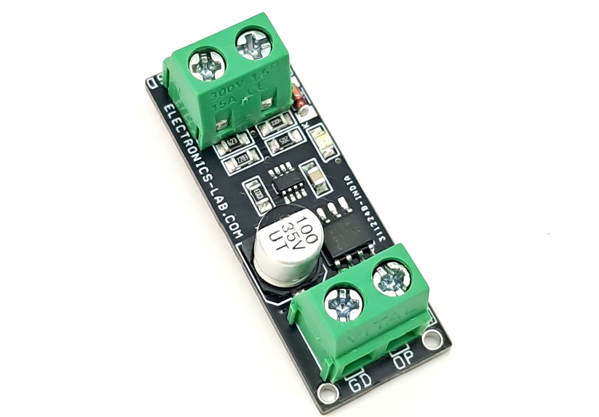
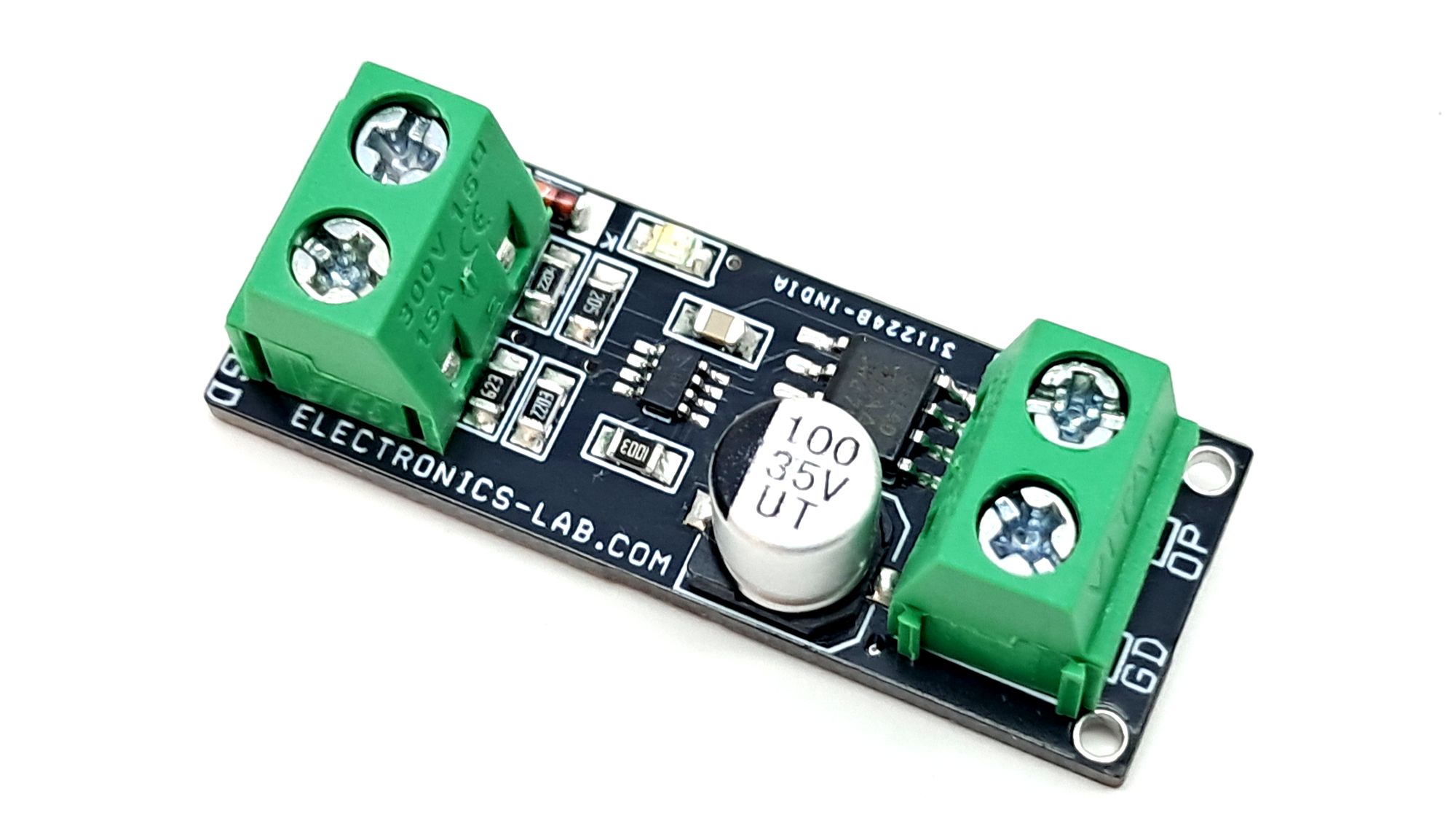
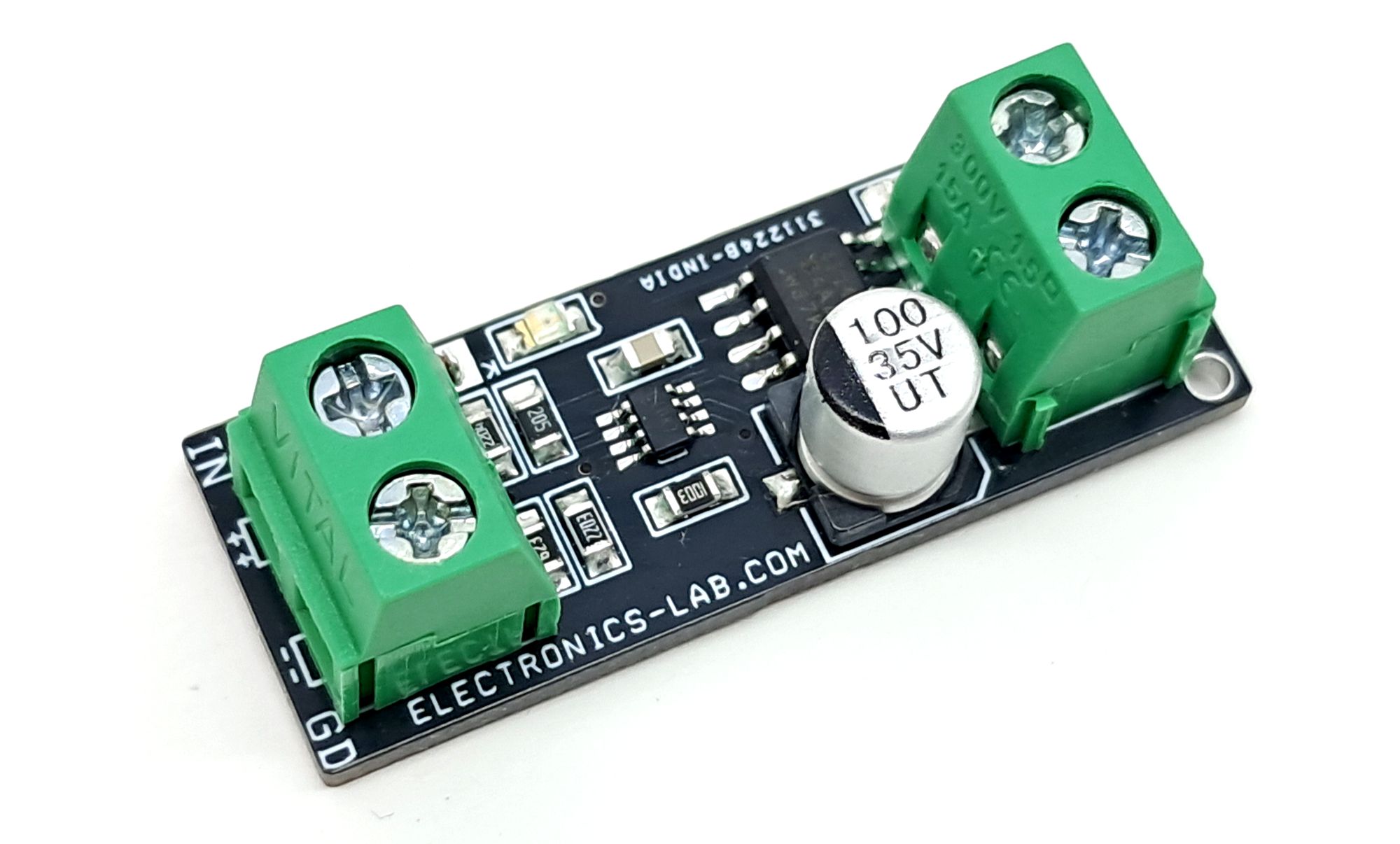
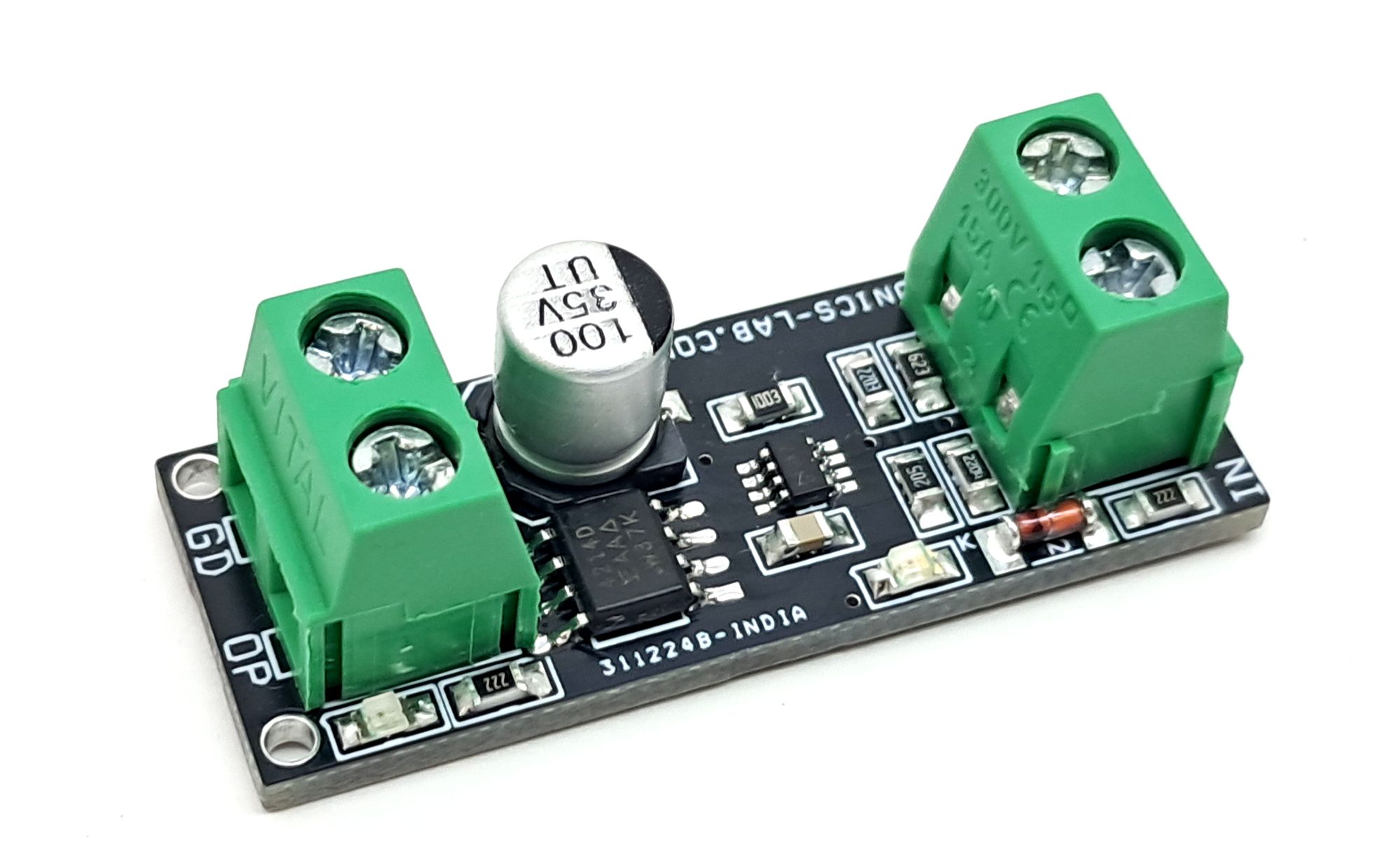
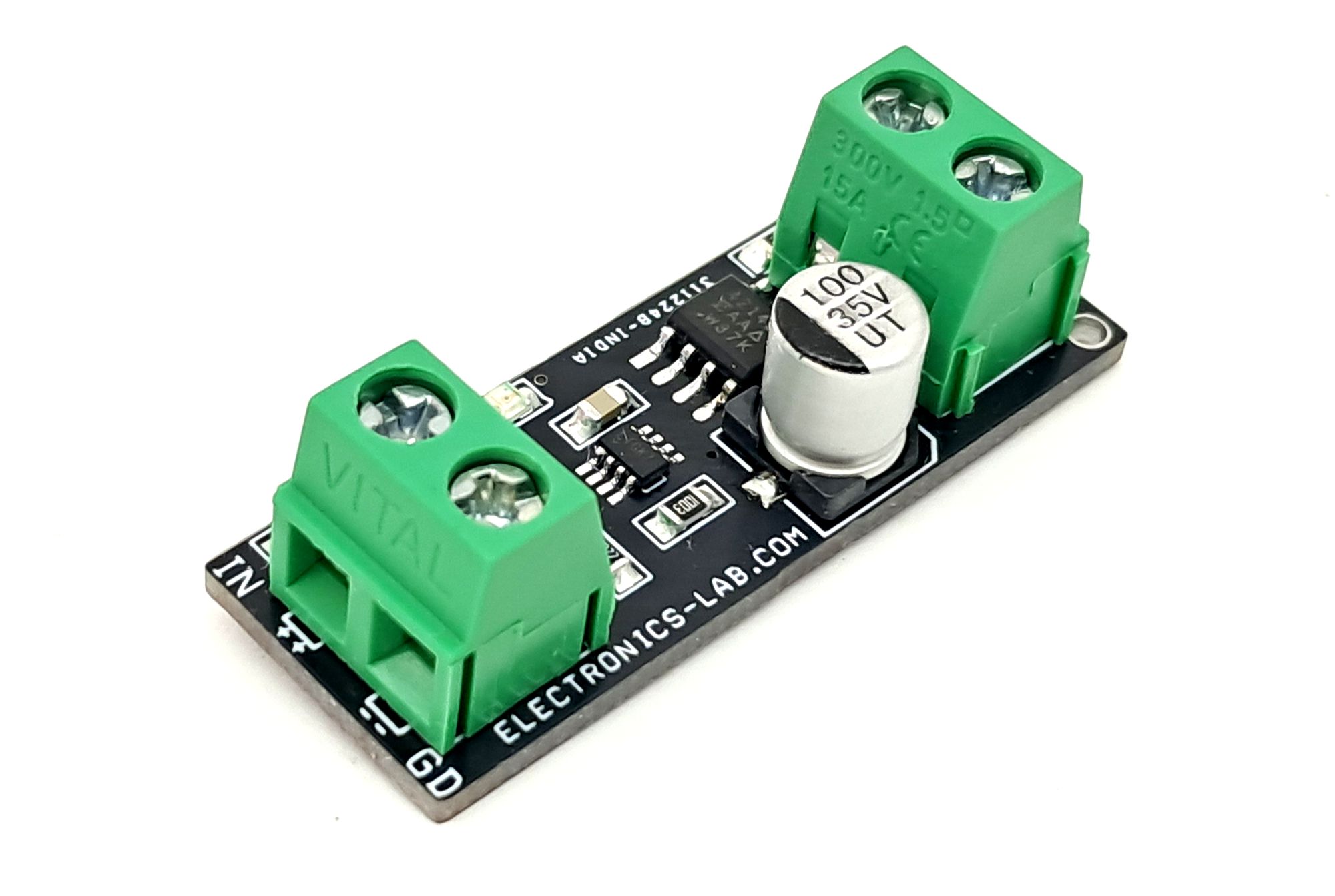
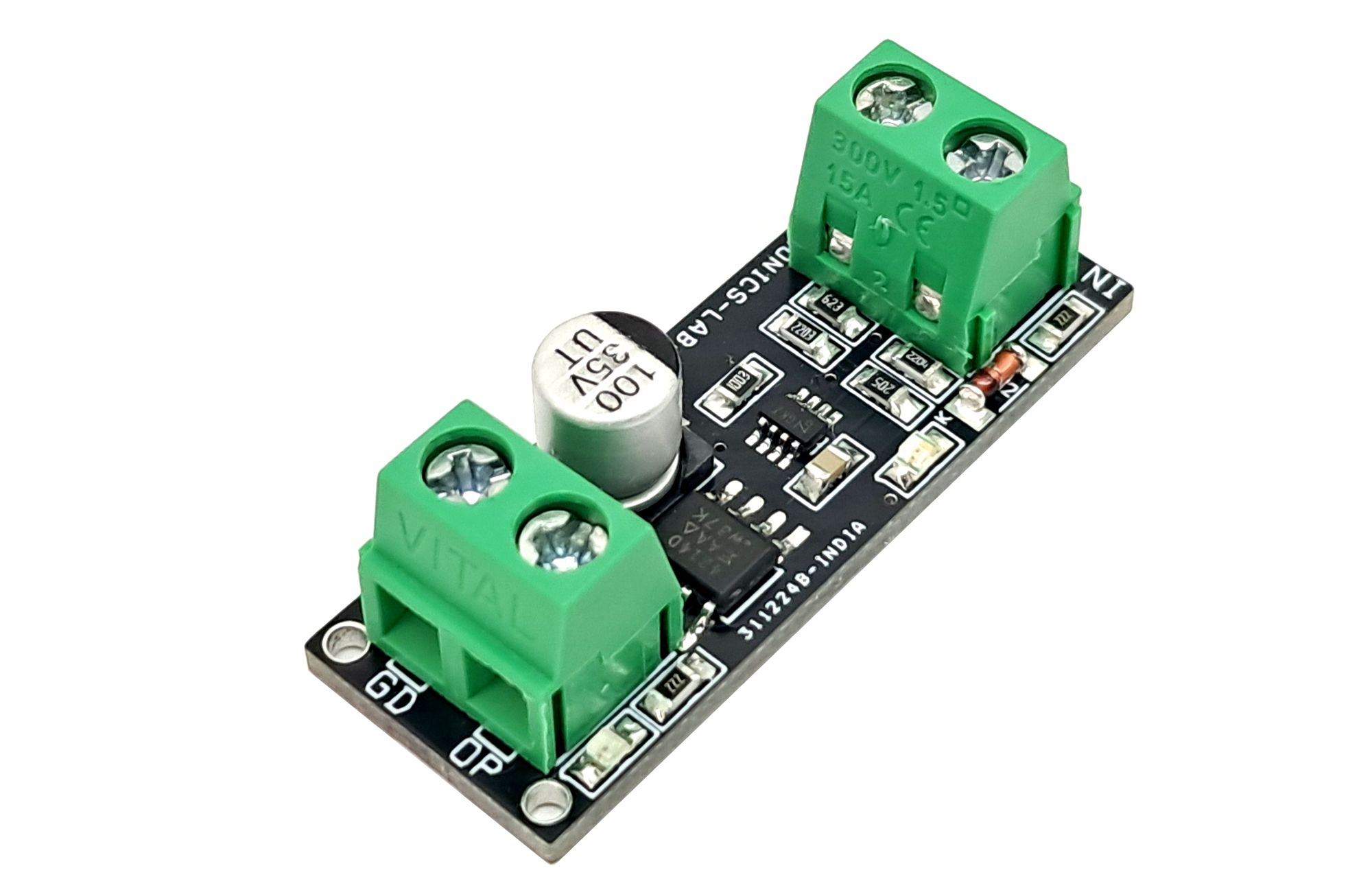
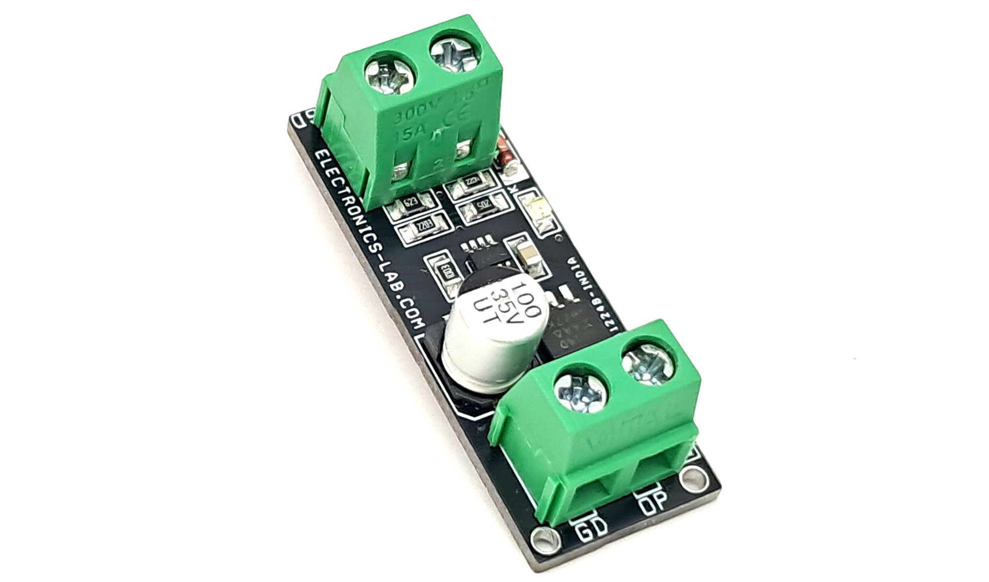
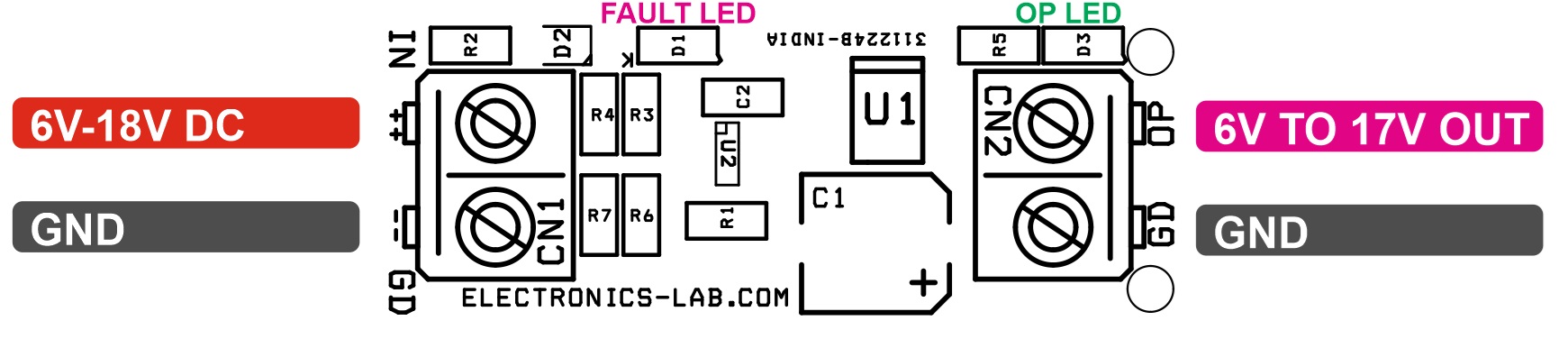
Connections
- CN1: Pin 1 = DC Input, Pin 2 = GND
- CN2: Pin 1 = DC Output, Pin 2 = GND
- D1: Fault LED
- D3: Output Power LED
Schematic
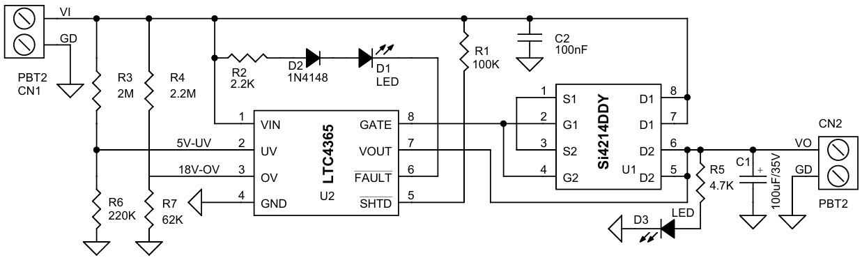
Parts List
| NO. | QNTY. | REF. | DESC. | MANUFACTURER | SUPPLIER | SUPPLIER PART NO |
|---|---|---|---|---|---|---|
| 1 | 2 | CN1,CN2 | 2 PIN SCREW TERMINAL PITCH 5.08MM | PHOENIX | DIGIKEY | 277-1247-ND |
| 2 | 1 | C1 | 100uF/35V ELECTROLYTIC | RUBYCON | DIGIKEY | 1189-1620-1-ND |
| 3 | 1 | C2 | 100nF/50V CERAMIC SMD SIZE 0805 | YAGEO/MURATA | DIGIKEY | |
| 4 | 2 | D1,D3 | LED RED SMD SIZE 0805 | OSRAM | DIGIKEY | 475-1278-1-ND |
| 5 | 1 | D2 | 1N4148 SMD | MICROCHIP | DIGIKEY | 1N4148UR-1-ND |
| 6 | 1 | R1 | 100K 5% SMD SIZE 0805 | YAGEO/MURATA | DIGIKEY | |
| 7 | 1 | R2 | 2.2K 5% SMD SIZE 0805 | YAGEO/MURATA | DIGIKEY | |
| 8 | 1 | R3 | 2M 1% SMD SIZE 0805 | YAGEO/MURATA | DIGIKEY | |
| 9 | 1 | R4 | 2.2M 1% SMD SIZE 0805 | YAGEO/MURATA | DIGIKEY | |
| 10 | 1 | R5 | 4.7K 5% SMD SIZE 0805 | YAGEO/MURATA | DIGIKEY | |
| 11 | 1 | R6 | 220K 1% SMD SIZE 0805 | YAGEO/MURATA | DIGIKEY | |
| 12 | 1 | R7 | 62K 1% SMD SIZE 0805 | YAGEO/MURATA | DIGIKEY | |
| 13 | 1 | U1 | Si4214DDY SOIC8 | VISHAY | DIGIKEY | SI4214DDY-T1-GE3CT-ND |
| 14 | 1 | U2 | LTC4365 | ANALOG DEVICE | DIGIKEY | 505-LTC4365CTS8#TRMPBFCT-ND |
Connections
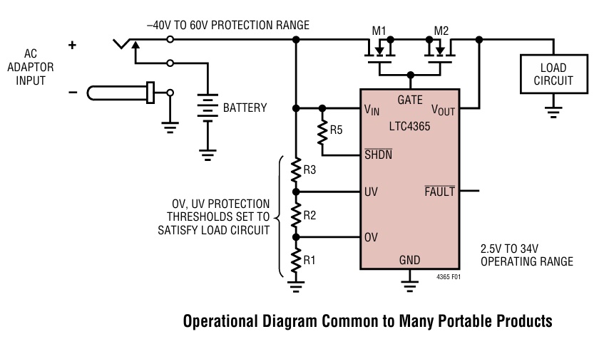
Application Diagram
LTC4365 Block Diagram
Gerber View
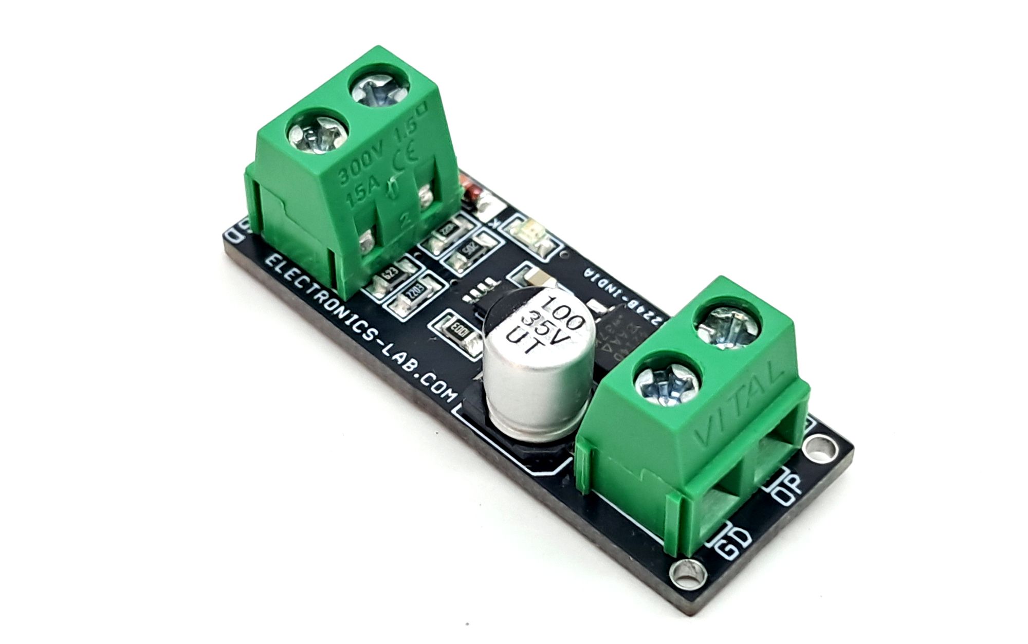
Photos