Serial-Input, Voltage-Output, 16-Bit DAC
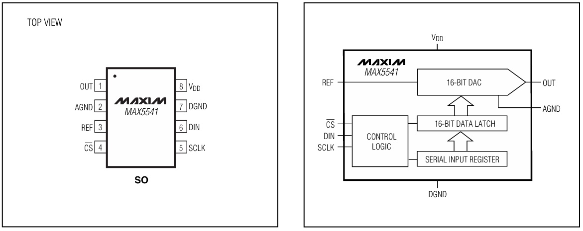
The MAX5541 is a 16-bit digital-to-analog converter (DAC). It's a low-power, unbuffered chip with a 3-wire serial interface, ideal for high-precision voltage output.
The project presented here uses the MAX5541 chip, a serial-input, voltage-output, 16-bit monotonic digital-to-analog converter (DAC) that operates from a single +5Vdc supply. Notably, the DAC output is unbuffered, resulting in a low supply current of 0.3mA and a minimal offset error of 1 LSB. The DAC output range spans from 0V to VREF, providing a wide range of voltage output options.
The DAC latch is designed to accept a 16-bit serial word, allowing for precise control over the output voltage. Additionally, a power-on reset (POR) circuit is integrated, which clears the DAC output to 0V in unipolar mode when power is initially applied. This ensures a stable and predictable startup sequence.
The 10MHz 3-wire serial interface is compatible with SPI, QSPI, and MICROWIRE protocols, enabling seamless communication with a wide range of microcontrollers and other devices. Furthermore, the interface can be directly connected to optocouplers, making it suitable for applications that require isolation.
To provide a stable reference voltage, the REF3025 chip is used, which supplies a precise 2.5V reference voltage to the DAC. This ensures that the DAC output is accurate and reliable, making it suitable for a variety of applications that require high-precision voltage output.
The MAX5541 voltage-output, 16-bit digital-to-analog converter (DAC) offers 16-bit monotonicity with less than 1LSB differential linearity error. Serial-data transfer minimizes the number of package pins required. The MAX5541 is composed of two matched DAC sections, with a 12-bit inverted R-2R DAC forming the twelve LSBs and the four MSBs derived from fifteen identically matched resistors. This architecture allows the lowest glitch energy to be transferred to the DAC output on major-carry transitions. It also decreases the DAC output impedance by a factor of eight compare to a standard R-2R ladder, allowing unbuffered operation in medium-load applications.
Features
- Power Supply 5V DC
- Full 16-Bit Performance Without Adjustments
- Low Power: 1.5mW
- 1µs Settling Time
- On Bord Ref-Voltage Chip Output 2.5V (REF3025)
- Unbuffered Voltage Output Directly Drives 60kΩ Loads
- SPI/QSPI/MICROWIRE-Compatible Serial Interface
- Power-On Reset Circuit Clears DAC Output to 0V (unipolar mode)
- Schmitt Trigger Inputs for Direct Optocoupler Interface
- Header Connector for Serial Interface and output
- On Board Power LED
- PCB Dimensions: 20.85 x 15.92 mm
Digital Interface
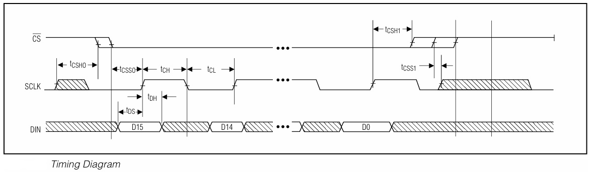
The MAX5541 digital interface is a standard 3-wire connection compatible with SPI/QSPI/MICROWIRE interfaces. The chip-select input (CS) frames the serial data loading at the data input pin (DIN). Immediately following CSs high-to-low transition, the data is shifted synchronously and latched into the input register on the rising edge of the serial-clock input (SCLK). After 16 data bits have been loaded into the serial input register, it transfers its contents to the DAC latch on CSs low-to-high transition (Figure 2). Note that if CS does not remain low during the entire sixteen SCLK cycles, data will be corrupted. In this case, reload the DAC latch with a new 16-bit word.
External Reference
The MAX5541 operates with external voltage references from 2V to 3V. The reference voltage determines the DACs full-scale output voltage REF3025 chip provides 2.5V reference.
Power-On Reset
The MAX5541 has a power-on reset (POR) circuit to set the DACs output to 0V in unipolar mode when VDD is first applied. This ensures that unwanted DAC output voltages will not occur immediately following a system power-up, such as after power loss In bipolar mode, the DAC output is set to -VREF.
Unbuffered Operation
Unbuffered operation reduces power consumption as well as offset error contributed by the external output buffer. The R-2R DAC output is available directly at OUT, allowing 16-bit performance from +VREF to AGND without degradation at zero-scale. The DAC’s output impedance is also low enough to drive medium loads (RL> 60kΩ) without degradation of INL or DNL, only the gain error is increased by externally loading the DAC output.
Digital Inputs and Interface Logic
The digital interface for the 16-bit DAC is based on a 3wire standard that is SPI/QSPI/MICROWIRE–compatible. The three digital inputs (CS, DIN, and SCLK) load the digital input data serially into the DAC. All of the digital inputs include Schmitt-trigger buffers to accept slow-transition interfaces. This means that optocouplers can interface directly to the MAX5541 without additional external logic. The digital inputs are TTL/ CMOS-logic compatible.
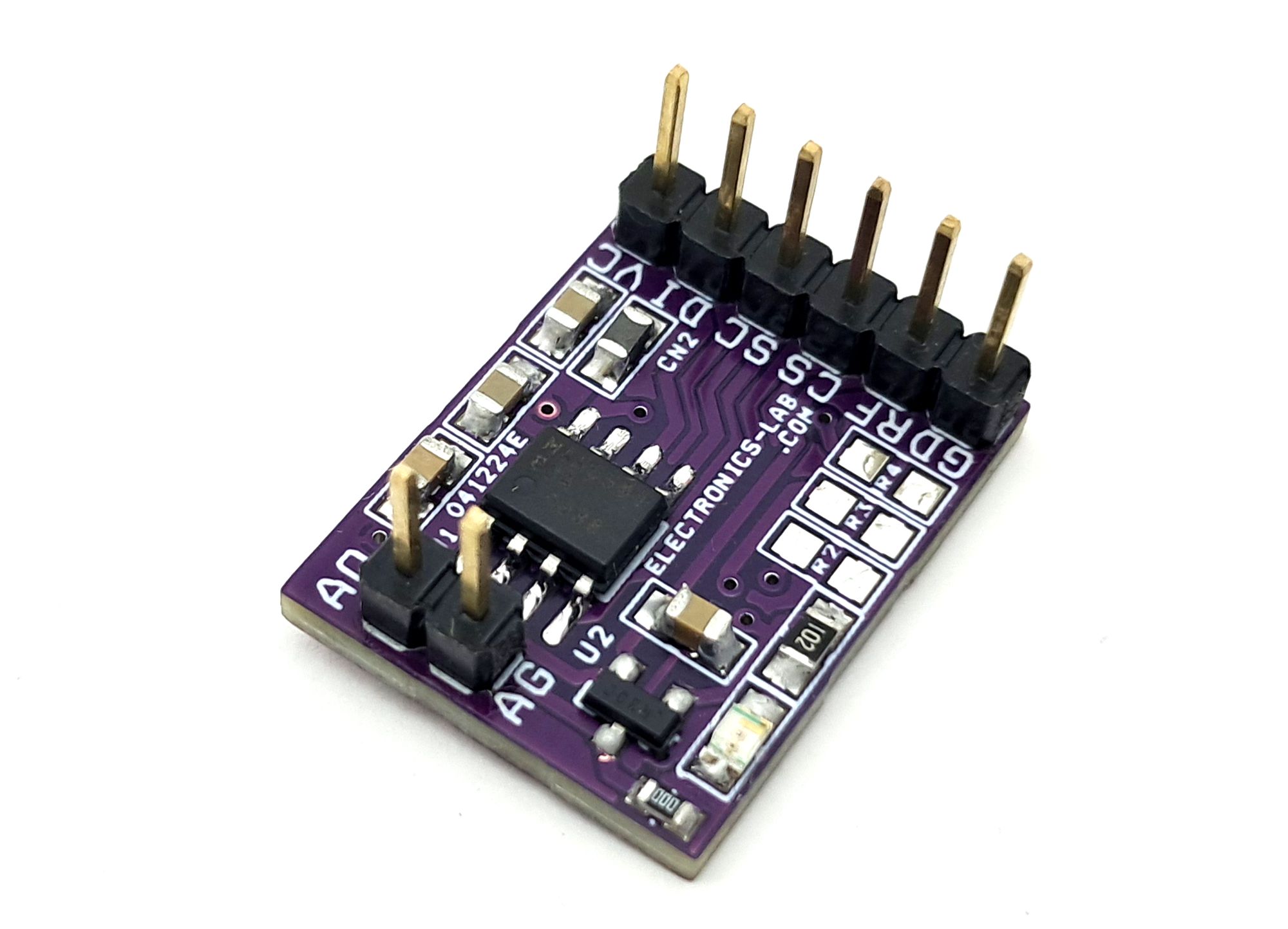
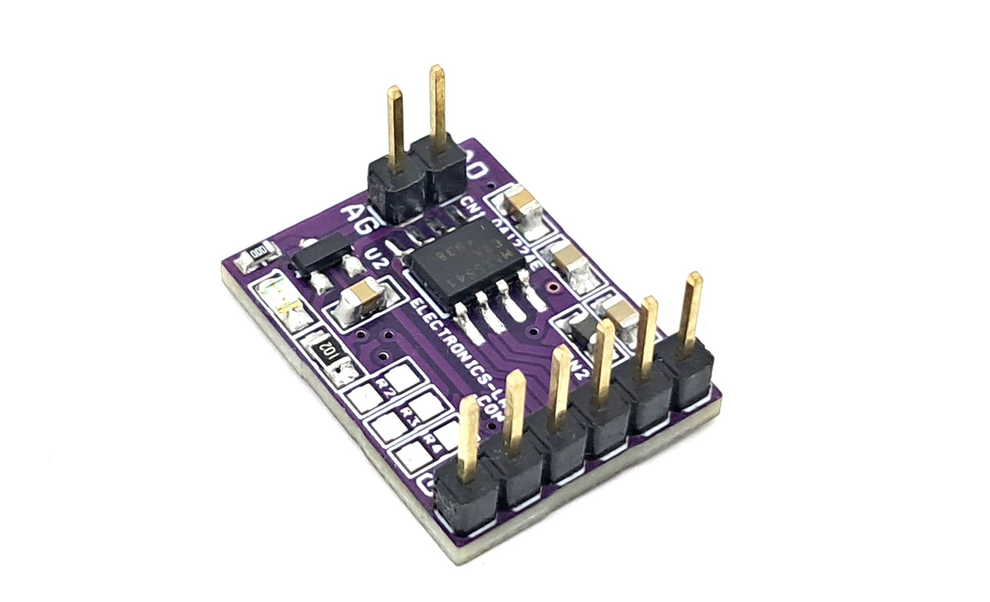
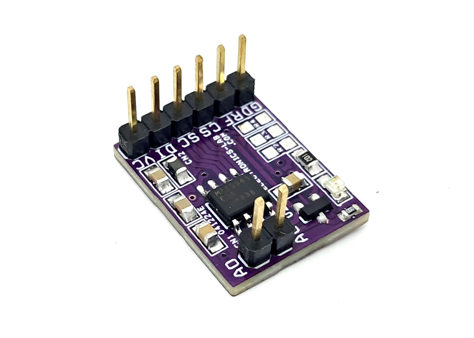
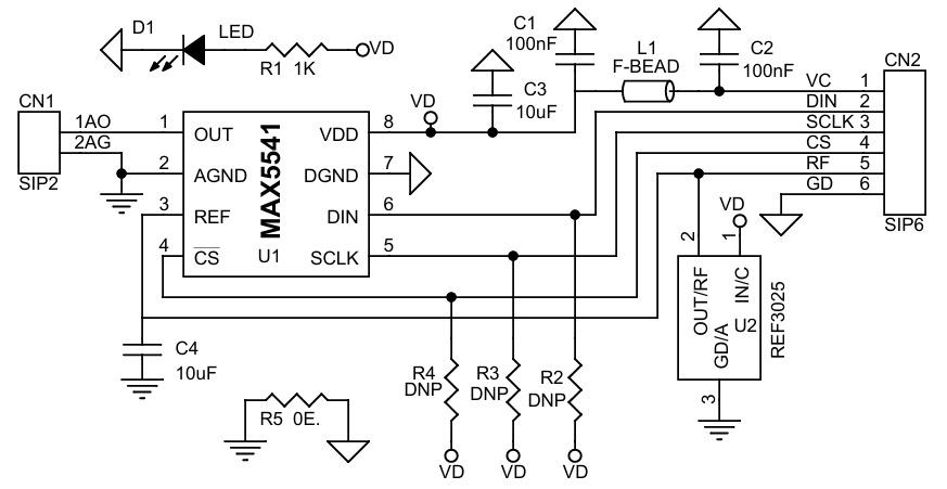
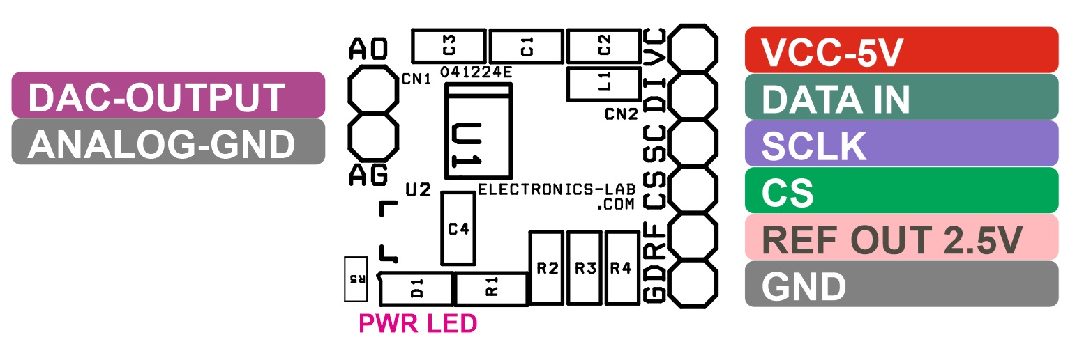
Connections
- CN1 DAC (Analog Output): Pin 1 = Analog Voltage Output, Pin 2 = Analog GND
- CN2 Interface & Power: Pin 1 = VCC 5V DC, Pin 2 = DIN, Pin 3 = SCLK, Pin 4 = CS, Pin 5 = Reference Output 2.5V, Pin 6 = GND
- D1: Power LED
Schematic
Parts List
| NO | QNTY. | REF | DESC. | MANUFACTURER | SUPPLIER | SUPPLIER PART NO |
|---|---|---|---|---|---|---|
| 1 | 1 | CN1 | 2 PIN MALE HEADER PITCH 2.54MM | WURTH | DIGIKEY | 277-1247-ND |
| 2 | 1 | CN2 | 6 PIN MALE HEADER PITCH 2.54MM | WURTH | DIGIKEY | 732-5319-ND |
| 3 | 2 | C1,C2 | 100nF/50V CERAMIC SMD SIZE 0805 | YAGEO/MURATA | DIGIKEY | |
| 4 | 2 | C3,C4 | 10uF/25V CERAMIC SMD SIZE 0805 | YAGEO/MURATA | DIGIKEY | |
| 5 | 1 | D1 | LED RED SMD SIZE 0805 | OSRAM | DIGIKEY | 475-1278-1-ND |
| 6 | 1 | L1 | FERRITE BEAD 600OHM SMD SIZE 0805 | LAIRD | DIGIKEY | 240-2390-1-ND |
| 7 | 1 | R1 | 1K 5% SMD SIZE 0805 | YAGEO/MURATA | DIGIKEY | |
| 8 | 3 | R2,R3,R4 | DNP | |||
| 9 | 1 | R5 | 0E SMD SIZE 0805 | YAGEO/MURATA | DIGIKEY | |
| 10 | 1 | U1 | MAX5541 SOIC8 | ANALOG DEVICE | DIGIKEY | MAX5541CSA+-ND |
| 11 | 1 | U2 | REF3025 SOT23-3 | TI | DIGIKEY | 296-26322-1-ND |
Connections
Pinout
Timing Diagram
Gerber View
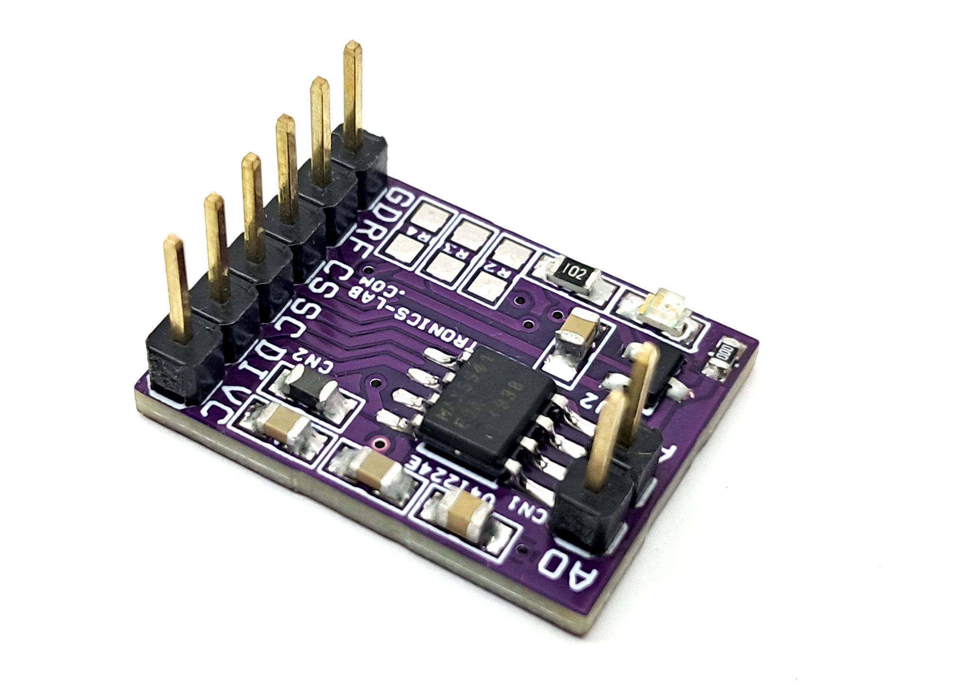
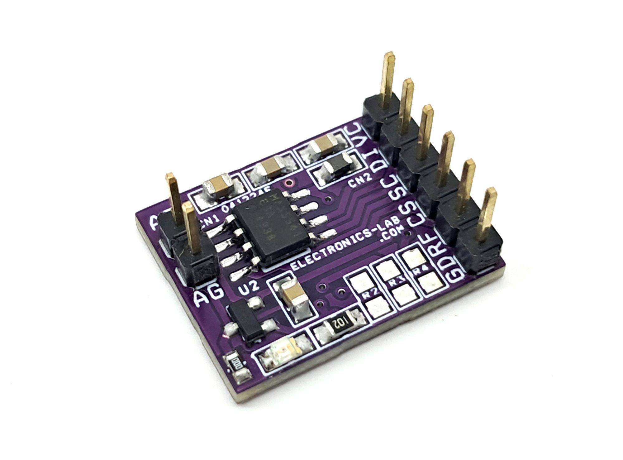
Photos