Rambus Addresses AI Data Center Power Constraints With SOCAMM2 Chipset
The new server module chipset comprises voltage regulators and an SPD Hub, enabling LPDDR5X memory to scale reliably within modular AI server architectures.
AI infrastructure demands heightened data rates and improved power efficiency, steering architectural interest toward low-power memory alternatives. While LPDDR memory delivers excellent power efficiency through lower operating voltages and high per-pin data rates, its use was previously restricted because DRAM devices had to be soldered directly to the motherboard to maintain signal integrity over short distances. However, placing LPDDR on conventional slotted server modules lengthens routing distances, which introduces noise and signal degradation at high frequencies.
To bridge this gap, the JEDEC-standard SOCAMM2 architecture implements a compact, low-profile module using compression-attach technology. This structural configuration mounts close to the processor to preserve short signal paths. Rambus has developed a dedicated server module chipset specifically to support this transition, providing the essential control, telemetry, and power delivery architecture required to stabilize LPDDR5X operations within modular data center hardware.
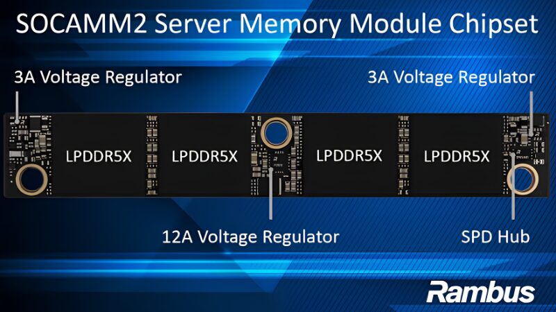
The SOCAMM2 server module chipset is designed to bring high-bandwidth, power-efficient LPDDR5X memory to AI data centers. Image used courtesy of Rambus
LPDDR-Based SOCAMM2 Chipset
The newly introduced SOCAMM2 server chipset enables the reliable operation of LPDDR5X-based server memory modules at maximum data rates of up to 9.6 Gb/s. The silicon solution integrates two distinct synchronous step-down DC-DC voltage regulators along with a centralized control hub.
The primary component is a 12 A voltage regulator, designated P2815Gxx, which incorporates a low-on-resistance power MOSFET. It utilizes a constant-on-time (COT) control architecture to enable fast transient responses and seamless mode transitions, maximizing efficiency during light-load operations. The regulator also features a programmable valley-current limit and an integrated soft-start function to mitigate inrush current during startup.
The secondary power component is a 3 A voltage regulator, part number P2813Gxx, operating at a 750 kHz switching frequency with integrated 100 mΩ and 60 mΩ FETs. Both regulators convert higher input supply voltages down to the sub-1-volt rails needed by the LPDDR components, mitigating the risks of voltage variation associated with long, lossy motherboard traces.
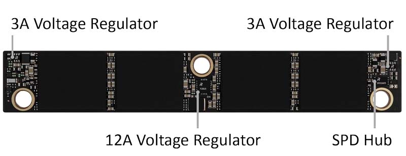
The chipset includes 12 A and 3 A voltage regulators and an SPD Hub. Image used courtesy of Rambus
Telemetry and system communications are managed by the SPD1605Gxx SPD Hub. This component features an integrated temperature sensor and supports I3C communication, enabling the host system to retrieve critical data for precise thermal telemetry and memory module configuration.
System Optimization and Hardware Applications
By localizing power management and control functions directly on the memory module substrate, this chipset architecture improves signal and power integrity across advanced server memory subsystems. Electrical engineers can leverage these components to design removable, upgradable server memory options that offer the power-saving characteristics of mobile hardware alongside enterprise-grade serviceability. Potential deployment configurations for these chipsets include next-generation AI server platforms, high-performance computing data centers, and thermally constrained, liquid-cooled processing environments that require high-bandwidth memory scalability without exceeding strict hardware power budgets.


