
Renesas Debuts Dual-Side-Cooled 650V GaN FET for 800V Data Centers
Housed in a compact 8x8 mm package that sheds heat from both sides, the 20 mω device targets the power-dense conversion stages of 800V AI rack architectures.
AI racks are swallowing power at a startling clip, and the boards that feed them tend to run out of two things well before they hit electrical limits: room and thermal headroom. Renesas has responded with the TP65H020G4PLSGBD, a 650V gallium nitride FET that the company describes as the first to offer dual-side cooling. Rack power is climbing from roughly 120 kW toward the megawatt scale, and this part targets 800V HVDC distribution schemes. Samples are going out now to major AI data center OEMs and ODMs, with mass production planned for mid-2027.
Heat Out Both Sides, Footprint Down
The device arrives in an 8 x 8 mm PQFN package, a footprint 57% smaller than the existing 10 x 15 mm TOLT package. Conventional top-side-cooled parts push their heat in a single direction; this one releases it from the top and the bottom alike, which Renesas says trims top-side thermal impedance by 10%. The datasheet puts junction-to-case thermal resistance at 0.36 °C/W through the top and 2.8 °C/W through the bottom. Because major AI infrastructure customers defined the package together, it follows an industry-standard footprint, leaving buyers room to source from more than one vendor.
Normally Off, Easy to Drive
Built on the Gen IV Plus platform, the part pairs a high-voltage depletion-mode GaN high-electron-mobility transistor with a low-voltage silicon MOSFET. The GaN die provides switching speed; the silicon device provides normally-off operation and compatibility with standard gate drivers. It requires no negative gate bias, has a typical threshold of 4V, and recommends a 9V on-state drive. Typical on-resistance is 20 mω (25 mω max), continuous drain current reaches 92 A at a 25°C case temperature, and the junction is rated from -55°C to +150°C. Typical gate charge is 19.6 nC and output charge is 221 nC, and the built-in freewheeling diode shows negligible reverse recovery charge, making MHz switching practical and shrinking passive components. Blocking capability is 650V, with transient excursions to 900V tolerated for under 10 µs.
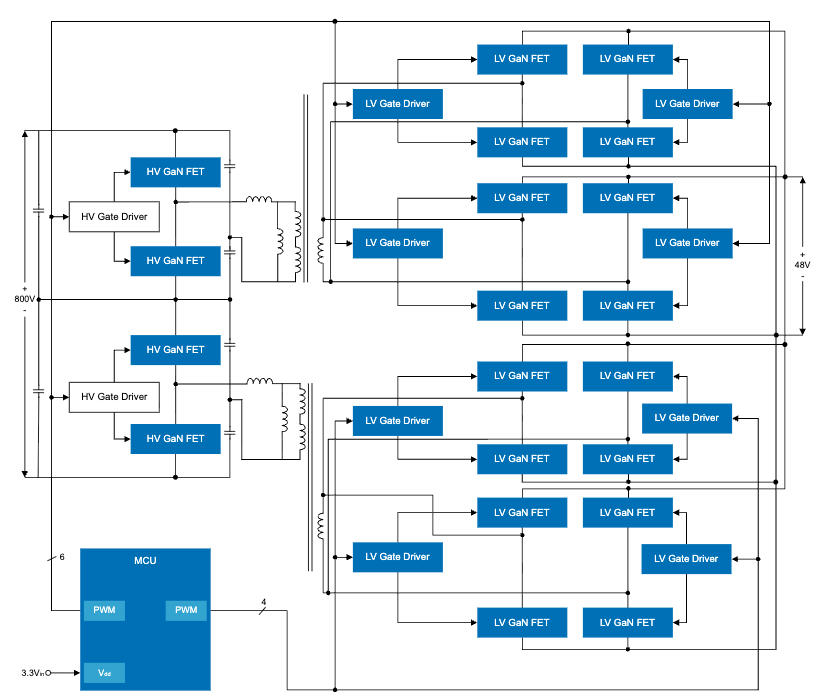
Two stacked primary-side half-bridges feed separate transformers, whose secondaries combine into a single 48V output. Image used courtesy of Renesas
Reference Designs and Target Stages
Renesas points the device at the 800V DC/DC intermediate bus converter stage, which steps down to 48V, 12V, or 6V, as well as the sidecar power rack’s battery backup and capacitor bank (CBU) stages. A 6 kW, 800V-to-48V LLC DC transformer reference design, controlled by an RA6T3 MCU, reaches 2.6 kW/in³. Per-module testing measured full-load efficiency 0.21% higher than an equivalent TOLT-based board, and the smaller package also saves PCB space while allowing a better-matched layout across the FETs. Reference designs for 800V-to-12V and 6V conversion use the same platform. Pairing the FET with Renesas AUX controllers, gate drivers, and MCUs rounds out a single-vendor path for teams moving to 800V. The company will show the device at OCP Global Summit in San Jose, October 12-15.
Taken together, the TP65H020G4PLSGBD trades a larger, one-sided thermal path for a smaller, two-sided one, all without asking designers to abandon the silicon gate drivers they already know. Data center power is the headline use, but the product page also lists telecom power supplies, photovoltaic inverters, uninterruptible power supplies, e-mobility charging, and battery energy storage systems as targets. Anyone wrestling with density and heat in a high-voltage converter will probably want to watch how the mid-2027 production ramp unfolds.


