STMicroelectronics Launches MPUs for Cost and Power-Constrained Designs
The STM32MP21 MPUs feature a 1.5 GHz Arm Cortex-A35 core and a 300 MHz Cortex-M33 core, offering high-performance, efficiency, and security in industrial applications and edge devices.
STMicroelectronics has introduced the STM32MP21 microprocessors (MPUs), extending its STM32MP2 family with devices optimized for cost-sensitive edge computing deployments. The multi-variant lineup targets applications in industrial automation, smart infrastructure, and connected devices where processing capability must be balanced against power budget and system cost constraints.
STMicroelectronics has priced its new STM32MP21 MPUs from $5.70 to $8.50 for units of 1000. Image used courtesy of STMicroelectronics
Asymmetric Multiprocessing Architecture
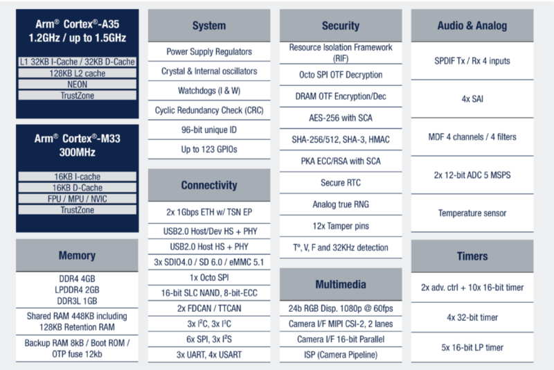
The STM32MP21 MPUs implement an asymmetric multiprocessing architecture combining a 64-bit Arm Cortex-A35 core operating at 1.5 GHz with a 32-bit Cortex-M33 core running at 300 MHz. Both cores incorporate Arm TrustZone technology for hardware-enforced security domain separation.
The dual-core configuration enables partitioning of computational workloads and real-time control functions. The Cortex-M33 can independently handle boot sequences and time-critical operations while the Cortex-A35 remains in a low-power state, reducing wake-up latency from power-saving modes. This architecture supports up to 456 KB of internal SRAM distributed across multiple domains, including 256 KB AXI SYSRAM, 64KB AHB SRAM, and 128KB AHB SRAM with ECC in the backup domain.
External memory support encompasses DDR3L-1600, DDR4-1600, and LPDDR4-1600 configurations with 16-bit bus widths, accommodating up to 4 GB of system memory. The inclusion of DDR3L support provides flexibility in addressing supply chain constraints affecting DDR4 and LPDDR4 availability.
Block diagram of the STM32MP215C/F MPU. Image used courtesy of STMicroelectronics
Integrated Connectivity and Imaging
The STM32MP21 MPUs integrate two Gigabit Ethernet interfaces supporting TSN protocols, enabling deterministic communication for industrial control applications. TSN features include IEEE 1588v2 hardware acceleration for time synchronization, supporting applications requiring bounded latency and synchronized operation across distributed systems. Interface options include MII, RMII, and RGMII physical layer connections.
The MPU’s machine vision capabilities are addressed through two camera interfaces. The primary interface supports MIPI CSI-2 with two data lanes operating at up to 2.5 Gbit/s each, handling 5-megapixel resolution at 30 fps. An integrated lite-ISP provides demosaicing, downscaling, cropping, and three pixel pipelines for RawBayer, RGB, YUV, and JPEG formats. The secondary camera interface handles 8-to-14-bit parallel data at up to 80 MHz for 1-megapixel capture at 15 fps.
The STM32MP21’s display output is managed by an LCD-TFT controller supporting up to FHD resolution at 60 fps with 24-bit parallel RGB888 output. The controller provides three layers, including a secure layer, with YUV format support. Additional peripheral complement includes three I3C interfaces at 12.5 Mbit/s, six SPI ports, seven UART/USART channels, and three SDMMC interfaces supporting up to 8-bit configurations.
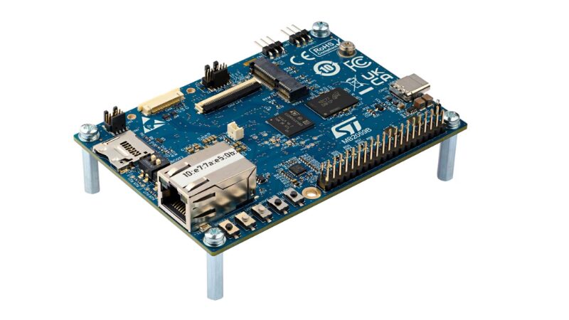
To begin prototyping and development, STMicroelectronics offers the STM32MP215F-DK discovery kit. Image used courtesy of STMicroelectronics
Security Architecture and System Integration
The STM32MP21 targets SESIP Level 3 certification, in line with the EU Cyber Resilience Act requirements. The security architecture implements multiple layers, including secure boot verification, dual cryptographic processors with side-channel attack countermeasures, and hardware-based RSA and ECC operations. On-the-fly DDR encryption protects external memory contents, while OTFDEC provides similar protection for Octo-SPI flash memory.
ST’s proprietary resource-isolation framework extends TrustZone protection across memory and peripheral access, preventing unauthorized resource tampering. The architecture includes dual HASH, along with two true random number generators for cryptographic operations.
Package options for the MPU range from 8 mm × 8 mm 225-pin VFBGA for high-density designs to 14 mm × 14 mm 289-pin TFBGA for cost-optimized 4-layer boards. The 10 mm × 10 mm 361-pin VFBGA maintains pin compatibility across the entire STM32MP2 lineup, and the STPMIC2L companion power management IC integrates required power rails for the MPU and DRAM, simplifying board-level power distribution design.
Cost-Sensitive Edge Designs
The STM32MP21 MPUs address embedded systems that require moderate processing performance, with integrated connectivity and security features.
Industrial automation applications benefit from the TSN-capable Ethernet interfaces and real-time processing partitioning between cores. Machine vision systems for quality inspection, barcode scanning, and object recognition can leverage dual-camera interfaces and integrated ISP capabilities. Smart infrastructure deployments, including access control, environmental monitoring, and building automation systems, align with the processor’s peripheral set and security architecture.
The MPU’s combination of DDR3L support, multiple package options, and cost positioning targets systems where component availability and total system cost constrain design choices while maintaining functional requirements for connectivity, processing, and security certification.


