Texas Instruments Expands Automotive Logic Devices With Multi-Function Gates
The configurable logic gates feature three independent channels with Schmitt-trigger inputs, targeting signal conditioning in automotive applications.
Texas Instruments has introduced two automotive-grade configurable logic devices, the SN74AHC3G99-Q1 and SN74AHCT3G99-Q1, designed to consolidate multiple discrete logic functions into a single component. Both devices feature three independent configurable gates with three-state outputs, each implementing the Boolean function. By appropriately connecting the four inputs per channel, engineers can configure each gate to perform 12 different logic operations, including two-to-one multiplexers, two-input AND, OR, NAND, NOR, XOR, and XNOR gates, and Schmitt-trigger buffers or inverters.
Texas Instruments’ new ultra-configurable three-channel multi-function gates are AEC-Q100 qualified for automotive applications. Image used courtesy of Texas Instruments
Three-Channel Multiple-Function Gates
Texas Instruments’ SN74AHC3G99-Q1 and SN74AHCT3G99-Q1 configurable gates are AEC-Q100 qualified for automotive applications with a device temperature grade 1 rating, supporting operation from -40°C to 125°C. Both variants achieve HBM ESD classification level 2 at ±2000 V and CDM classification level C4B at ±1000 V. The devices’ latch-up performance exceeds 100 mA per JESD 17, addressing robustness requirements in automotive environments.
All inputs incorporate Schmitt-trigger architecture, providing hysteresis to reject slow-edged or noisy signals. At 5 V operation, the SN74AHC3G99-Q1 exhibits a typical hysteresis of 0.8 V, while the SN74AHCT3G99-Q1 provides 0.7 V typical hysteresis. This input conditioning eliminates the need for external signal-cleanup circuitry in applications that require switch debouncing, long cable runs, or interfacing with sensors that produce slow transitions.
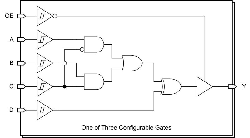
Functional block diagram of the automotive ultra-configurable three-channel multi-function gates. Image used courtesy of Texas Instruments
Voltage Range and Input Compatibility Differentiate Variants
The primary distinction between the two devices lies in the supply voltage range and input compatibility. The SN74AHC3G99-Q1 operates across a 2 V to 5.5 V supply range with standard CMOS input thresholds. At 5 V, it specifies positive-going threshold voltages of 3.3 V minimum and 3.5 V typical, and negative-going threshold voltages of 1.5 V minimum and 2.6 V typical.
The SN74AHCT3G99-Q1 variant operates from 4.5 V to 5.5 V and features TTL-compatible input thresholds specifically designed for interfacing with TTL logic families. At a 5 V supply, the positive-going threshold is 1.3 V minimum to 2 V maximum, while the negative-going threshold ranges from 0.5 V minimum to 1.3 V maximum. This compatibility allows direct connection to 5 V TTL outputs without level translation.
Both devices feature balanced CMOS three-state outputs capable of sourcing or sinking 8 mA at 5 V. The active-low output enable inputs provide independent control of each channel’s high-impedance state, facilitating bus architectures and power management schemes. Output voltage specifications at a 4.5 V supply show a minimum VOH of 3.8 V when sinking 8 mA and a maximum VOL of 0.44 V when sourcing 8mA.
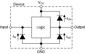
SN74AHC3G99-Q1 and SN74AHCT3G99-Q1 clamp diode structure. Image used courtesy of Texas Instruments
Propagation Delay and Package Options
Propagation delay performance differs between the variants. The SN74AHCT3G99-Q1 achieves maximum propagation delays of 11.7 ns at 5 V with a 50 pF load across the operating temperature range. The SN74AHC3G99-Q1 specifies a maximum delay of 21.8 ns under the same conditions. Both devices specify output disable times (tPLZ, tPHZ) below 6.4 ns and enable times (tPZL, tPZH) below 4.6 ns at 5V with 50 pF loading.
The static supply current for both devices is 0.3 nA typical and 40 µA maximum at 5.5 V, with all inputs at VCC or ground and no output loading. The SN74AHCT3G99-Q1 specifies an additional dynamic supply current parameter of 0.2 mA typical and 1.5 mA maximum when one TTL-compatible input is held at 3.4 V.
Both devices are available in three package options: 20-pin TSSOP (6.5 mm × 6.4 mm), 20-pin VSSOP (5.1 mm × 4.9 mm), and 20-pin VQFN (4.5 mm × 2.5 mm). The VQFN package features wettable flanks, which provide additional surface area for solder adhesion and facilitate automated optical inspection of solder joints. All three package types support tape-and-reel quantities of 3,000 to 5,000 units with NIPDAU lead finish and Level-1-260C-UNLIM moisture sensitivity rating.
Applications Target Automotive Signal Management
The configurability of Texas Instruments’ newest devices addresses common automotive signal-conditioning requirements. Possible applications include combining power-good signals from multiple sources, combining enable signals, eliminating slow or noisy input signals via Schmitt-trigger conditioning, synchronizing inverted clock inputs, switch debouncing, error signal monitoring with reduced input count, data selection, and multiplexing operations.
The three-state output capability enables multiple devices to share common buses under coordinated control, reducing trace count in space-constrained automotive control modules. The Boolean function implementation allows a single gate to perform signal-gating operations, with one input serving as an enable and the others carrying data or control signals. Engineers can configure unused gates as simple Schmitt-trigger buffers to clean up signals elsewhere in the system, maximizing device utilization.


