
NXP RW610FML Module Brings Wi-Fi 6 and BLE 5.4 Connectivity
The RW610FML combines a 260 MHz Cortex-M33 MCU, dual-band Wi-Fi 6, BLE 5.4, 8 MB Flash, and advanced security in a compact module.
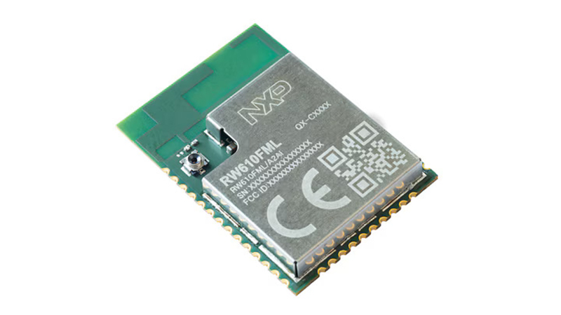
RW610FML wireless module
NXP Semiconductors recently unveiled the RW610FML, an innovative portable, ultra-low-power, standardised Wi-Fi 6 and Bluetooth Low Energy (BLE) 5.4 wireless communications module based on the organisation’s RW610 Arm Cortex-M33 microcontroller capable of supporting IEEE 802.11a/b/g/n/ac/ax and Bluetooth Low Energy (LE) protocols and aimed at low-power Internet of Things (IoT) devices.
The surface-mount module is designed for smart appliances, home automation, industrial gateways, and medical devices and integrates the 260 MHz Arm Cortex-M33 wireless SoC with 1.2MB of on-chip static RAM (SRAM), a quad serial peripheral interface (QSPI) supporting execute-in-place (XIP) from external flash, 8MB of on-module NOR flash, a built-in antenna, an RF matching circuit, and a crystal oscillator.
Previously, we covered the Murata Type 2FR/2FP IoT module, which also integrates the NXP RW610 SoC. It features security technologies such as EdgeLock Assurance and supports the Matter protocol. Feel free to check out this module as well.
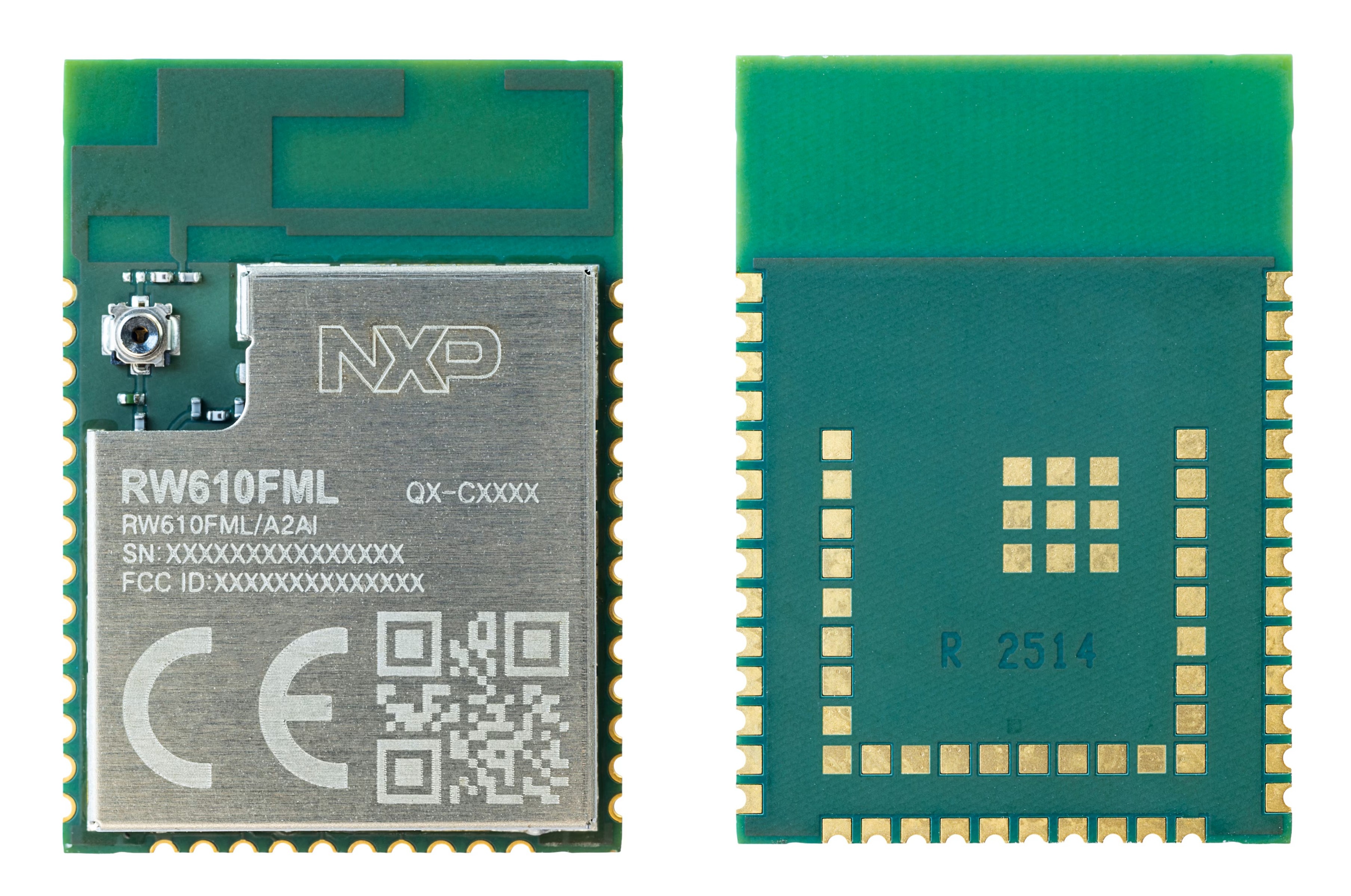
RW610FML wireless module top and bottom side
NXP RW610FML Wireless MCU Specifications:
- Wireless MCU: NXP RW610 wireless microcontroller
- Processor:
- 260 MHz Arm Cortex-M33 CPU
- Arm TrustZone-M security technology
- Memory:
- 1.2 MB embedded on-chip SRAM
- 8 MB integrated NOR Flash
- Wi-Fi Connectivity:
- Dual-band 2.4 GHz and 5 GHz Wi-Fi 6
- IEEE 802.11a/b/g/n/ac/ax compliant
- SISO operation
- Up to 20 MHz channel bandwidth
- Supports up to MCS9
- Peak data rate of up to 114 Mbps
- Bluetooth Connectivity:
- Bluetooth Low Energy (BLE)
- 2 Mbps high-speed mode
- Bluetooth LE Long-Range support
- Extended advertising capability
- External Memory and Storage:
- 2× FlexSPI interfaces for external NOR Flash and PSRAM
- Execute-in-Place (XIP) support
- SDIO 3.0 interface
- Integrated FlexSPI on-the-fly decryption engine for secure XIP execution from external Flash
- Display Interface: LCD interface
- Audio Interfaces:
- I²S / PCM
- Digital Microphone Interface (DMIC)
- Analog Peripherals:
- ADC
- DACAnalog Comparator (ACOMP)
- Digital Interfaces:
- USB
- UART
- I²C
- SPI
- GPIO
- SIM and Wireless Coexistence:
- Universal Subscriber Identity Module (USIM)
- Wireless Coexistence Interface 2 (WCI-2)
- Packet Traffic Arbitration (PTA)
- Debugging:
- JTAG
- Serial Wire Debug (SWD)
- Security:
- NXP EdgeLock security architecture
- Secure boot
- Secure debug
- Secure firmware updates
- Secure lifecycle management
- Hardware cryptographic acceleration
- Physically Unclonable Function (PUF) for secure key management
- Timers and PWM:
- SCTimer / PWM
- Micro-tick Timer (UTICK)
- Antenna: Integrated PCB antenna
- Host Interface: Castellated holes and pads for easy integration with host boards
- Package: Surface-mount LGA module
- Dimensions: 25.5 × 18 × 3.16 mm
- Weight: Approximately 1.51 g
- Operating Temperature: -40°C to 85°C
- Storage Temperature: -45°C to 95°C
- Moisture Sensitivity Level: MSL 3
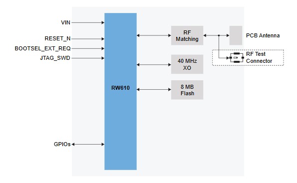
NXP RW610FML Block Diagram
Key Features:
- Wi-Fi 6 + Bluetooth LE: Combines dual-band Wi-Fi 6 and Bluetooth Low Energy connectivity in a compact wireless MCU module.
- High-performance processing: Features a 260 MHz Arm Cortex-M33 processor with TrustZone-M for secure embedded applications.
- Secure external memory execution: FlexSPI integrates an on-the-fly decryption engine, allowing applications to securely execute code directly from external Flash using XIP.
- Extensive peripheral connectivity: Provides USB, UART, I²C, SPI, GPIO, SDIO, LCD, audio, analog, and USIM interfaces for flexible system integration.
- Advanced security: EdgeLock security capabilities provide hardware-assisted protection for boot, firmware, debugging, cryptographic operations, and device lifecycle management.
- Flexible memory expansion: Dual FlexSPI interfaces support external NOR Flash and PSRAM for applications requiring additional storage and working memory.
- Integrated antenna design: The built-in PCB antenna simplifies wireless hardware integration and reduces external component requirements.
- Compact industrial-grade design: The LGA module measures just 25.5 × 18 × 3.16 mm and supports an operating temperature range of -40°C to 85°C.
NXP Semiconductors is also offering the FRDM-RW610FML module, a sleek and modular development board for accelerated prototyping of the RW610FML Wi-Fi 6 + Bluetooth LE combo module to streamline the development process. In conjunction with the FRDM-RW610FML, it gives straightforward access to the module’s GPIOs and peripherals, serial interfaces, and on-module flash memory.
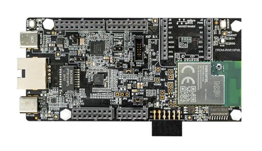
NXP FRDM-RW610FML Development Board
The module runs FreeRTOS or Zephyr OS RTOS and can be developed using MCUXpresso IDE, MCUXpresso for Visual Studio Code, IAR Embedded Workbench, or Keil MDK.
The RW610FML wireless MCU module and FRDM-RW610FML development board are currently listed as preproduction products. Pricing has not yet been released although with the part listed as in pre-production. More details including the preliminary RW610FML fact sheet can be found on the product page and in the press release.
Images used courtesy of NXP


