Toshiba Targets Automotive Power Safety With New Ideal Diode Controller
The TPD7110F features reverse-current blocking and reverse-connection protection, delivering safe power control in body control modules, head-up displays, and other automotive systems.
Redundant power rails are increasingly common in automotive electronics, particularly as systems take on more safety-critical roles. When two power sources feed the same rail, you need something to prevent backflow between them, and that’s where an ideal diode controller comes in.
Toshiba Electronics’ new TPD7110F handles that job while also guarding against several other failure modes automotive designers must account for.
Toshiba’s TPD7110F ideal diode controller for automotive systems. Image used courtesy of Toshiba Electronic Devices & Storage Corporation
The TPD7110F Ideal Diode Controller
Toshiba’s TPD7110F is a high-side N-channel MOSFET gate driver that functions as an ideal diode controller. It uses an internal charge pump with an onboard capacitor to drive the gate of an external N-channel MOSFET, creating an ideal diode configuration with low switching losses. The onboard capacitor is a practical detail: it eliminates the external bootstrap capacitor required by many competing designs, reducing component count and board space.
The device operates from 3 V to 32 V and is controlled via a logic-level IN pin. When the IN pin is high, the charge pump activates and turns the MOSFET on; when it goes low, the pump stops, and an off-driver pulls the gate down, keeping standby current to a typical 2 µA. During normal on-state operation, supply current is typically 100 µA.
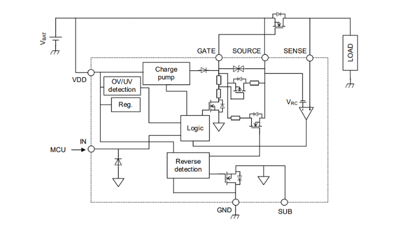
TPD7110F block diagram. Image used courtesy of Toshiba Electronic Devices & Storage Corporation
Protection Functions
The TPD7110F offers four protection modes. Reverse polarity protection handles battery connection errors up to -32 V by monitoring the VDD and GND terminals and disabling the MOSFET gate drive when a reverse connection is detected. The GND switch inside the IC also opens under this condition, preventing reverse current from entering through the ground pin.
Reverse current blocking works by monitoring the drain-source voltage across the external MOSFET via the SENSE and SOURCE pins. When the load-side voltage exceeds the supply-side voltage by 20 mV to 40 mV (the VRC threshold), the MOSFET is switched off to block current from flowing back toward the battery. This function can be disabled in designs where bidirectional current flow is intentional: for example, to enable energy recovery into the battery.
Undervoltage lockout trips below approximately 2.4 V, and overvoltage protection activates when VDD exceeds approximately 36 V (typical), both of which turn the MOSFET off until conditions return to normal.
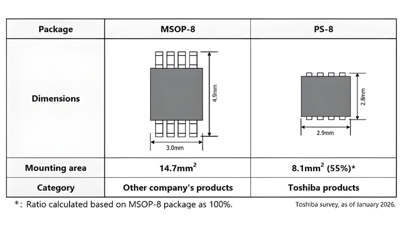
Toshiba compares its PS-8 package to a standard MSOP-8 package, highlighting a smaller footprint for space-constrained PCB designs. Image used courtesy of Toshiba Electronic Devices & Storage Corporation
Power Control in Automotive Systems
The TPD7110F is housed in Toshiba’s PS-8 package, measuring 2.9 mm × 2.8 mm. According to Toshiba, this footprint offers roughly half the mounting area of a conventional MSOP-8, which is a meaningful advantage in space-constrained PCB layouts. The device is rated for a junction temperature range of -40 °C to 125°C and meets AEC-Q100 reliability standards for automotive use.
Pairing two TPD7110F units with separate MOSFETs creates a redundant power supply architecture. Pairing one unit with back-to-back MOSFETs enables a controlled load switch. The device targets automotive systems, including body control modules, battery management systems, and head-up displays.


