


AI Compute Acceleration Startup Builds the Largest Chip Ever For Deep Learning Applications
To meet the ever-increasing computational demands of AI, California based AI startup, Cerebras Systems, just recently unveiled its very first announced element claimed to be the most massive AI chip ever made. With an astounding measurement of 46,225 mm2 (up to 56.7 times more than the largest graphics processing unit) and more than 1.2 trillion transistors, the Wafer-Scale Engine from Cerebras Systems is the largest semiconductor ever built for deep learning applications.
The Wafer-Scale Engine contains about 400,000 high performance, AI optimized Sparse Linear Algebra cores. This local memory fed cores are linked together by a fine-grained, high bandwidth, all-hardware, low latency mesh communication network at an interconnect speed of 100,000 Pb/s. Unlike other processors and GPUs that are produced on silicon wafers, Cerebras’ WSE is a single chip interconnected in a single wafer designed to handle all its transistors. The WSE also houses on-chip of 18Gb superfast and distributed SRAM memory among the cores in a single-level hierarchy. By way of comparison, the WSE has 3000 more on-chip memory and more than 10,000 times the memory bandwidth.
Designed for accelerating AI work, the company claims that its Wafer-Scale Engine can scale down the time it takes to process complex data from months to minutes.
“Every architectural decision was made to optimize performance for AI work. Designed from the ground up for AI work, the Cerebras WSE contains fundamental innovations that advance the state-of-the-art by solving decades-old technical challenges that limited chip size such as cross – reticle connectivity, yield, power delivery and packaging. The result is that the Cerebras WSE delivers, depending on workload, hundreds or thousands of times the performance of existing solutions at a tiny fraction of the power draw and space,”
says, CEO and Founder of Cerebras Systems, Andrew Feldman.
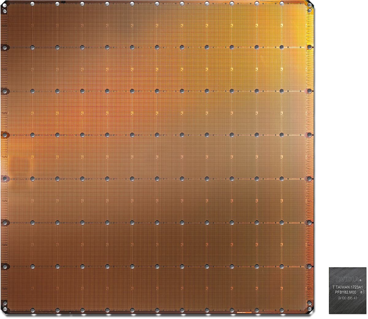
According to the company, bigger is better; the larger the chips, the less time it takes to process information and produce answers. The performance gain of the Wafer Scale Engine is largely due to its size. With a chip as big as the size of an iPad, the WSE is able to process information more quickly in less time, thus facilitating several AI paradigms like reducing the “time-to-insight” or “training time” within neural network loops. The speed at which a neural network loop is able to learn or train depends on the speed with which inputs move through the loop as such, the faster the inputs are processed through the feedback loop, the more inputs the loop receives per unit time and the faster the loop trains.
Due to its large silicon area, the WSE is able to provide more cores, more memory close to the cores that ensures that the cores are always occupied doing calculations, and more latency bandwidth between the cores for maximum efficiency. The programmable SLA cores are designed fundamentally to handle core neural network workload like TensorFlow, Pytorch and more.
In recent years, we have seen Artificial Intelligence rise from a state of obscurity to top-of-the-mind awareness because of the advances in deep learning. With WSE that help to train models in less time and with less energy, deep learning researchers should be able to explore more ideas, test hypothesis more quickly, use more data and solve new problems.
RELATED POSTS
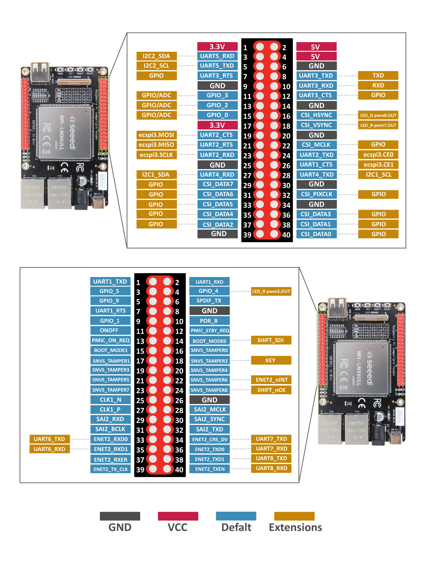 30 September, 2019 Seeed Opens Pre-Orders for NPi i.MX6ULL Dual-Ethernet Dev Board
 6 July, 2016 IN-4 Nixie Clock using ATmega168
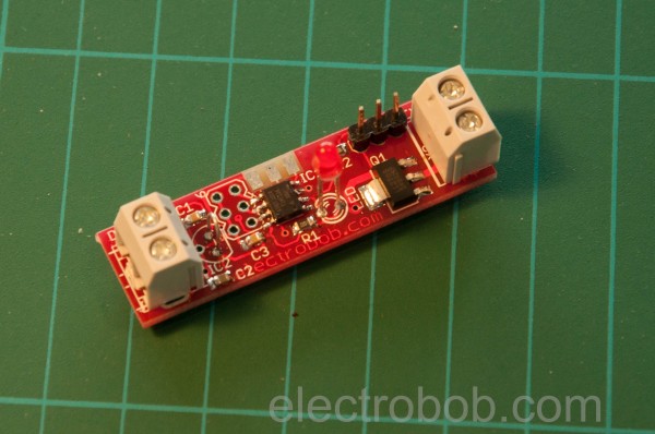 31 May, 2016 AutoResetRRR – Automatically reset routers/cameras/servers
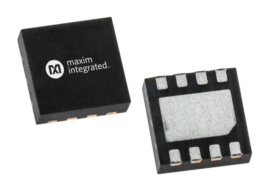 8 February, 2021 Maxim Integrated MAX38911 LDO Linear Regulators
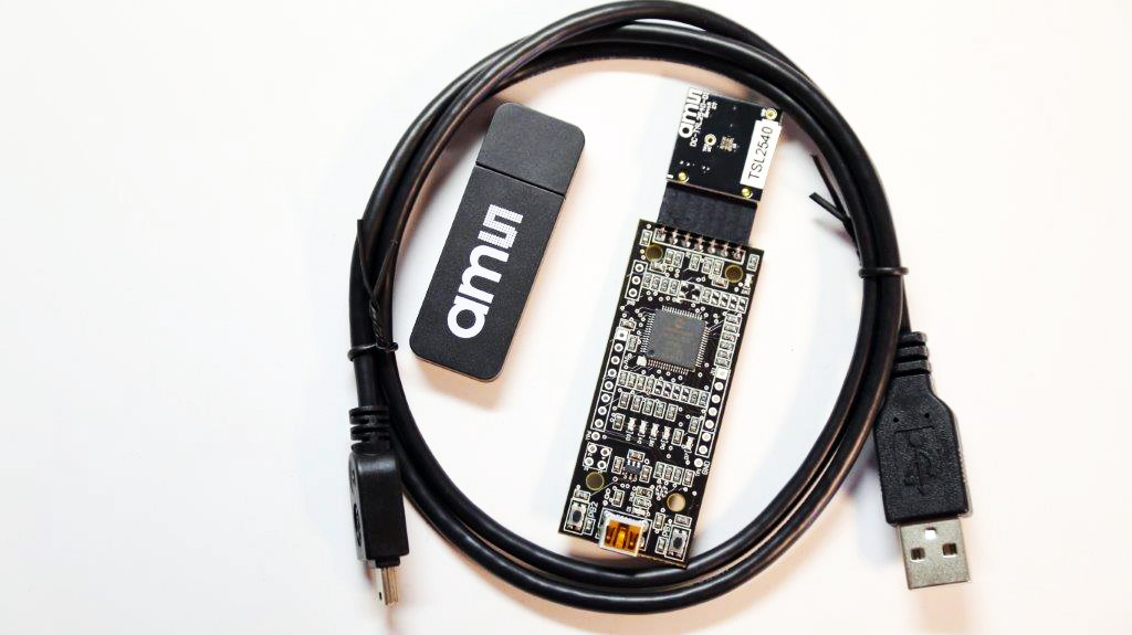 31 October, 2017 TSL2540 Ambient Light Sensor matches eye-response
 12 October, 2021 1-Cell Li-ion Battery Protection IC with Built-in Driver for High-side Nch FETs and Temperature Protection