Operational Amplifier Basics
Introduction This tutorial is an introduction to the Operational Amplifiers, also known as op-amps. The fundamental goal of op-amps is to amplify a voltage difference and it is the reason why we also describe them as differential amplifiers.
Introduction
This tutorial is an introduction to the Operational Amplifiers, also known as op-amps. The fundamental goal of op-amps is to amplify a voltage difference and it is the reason why we also describe them as differential amplifiers.
Op-amps have been invented the exact same year as the transistors (1947) and they were originally designed with vacuum tubes in order to perform basic mathematical operations. Mass-production only started in the ’50s when the op-amps were heavy, not reliable, and cost much. Not before the late ’60s were produced large amounts of transistor-based op-amps available for just a few $.
Nowadays, op-amps are one of the most used electronic components, their cost is only of a few cents of $, and thanks to their interesting properties they are used for many applications.
In the first section, we will present in detail the architecture and definitions surrounding op-amps. Moreover, we briefly discuss the internal circuitry of op-amps.
The second section focuses on the concept of the ideal op-amp which is a model describing the functioning of a perfect op-amp.
Real op-amps will be discussed in the third section where we will look into the differences that must be considered.
Presentation
An op-amp is usually represented as a triangle with 5 pins from which 4 are inputs and one is the output.
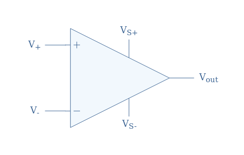
The output is labeled Vout and it is the pin where the output voltage is collected. V+ and V– are respectively the non-inverting and inverting inputs. VS+ and VS- are respectively the positive power supply and negative power supply rails.
We can note that in most of the op-amps representations, the power supply voltages and pins are not represented in order to simplify the drawing. Most of the time, the power configuration is just assumed or not relevant to perform calculations on a specific op-amp.
The internal circuitry of op-amps generally consists of a succession of bipolar or field-effect transistors and other passive components that are assembled in three distinct stages as shown in Figure 2:
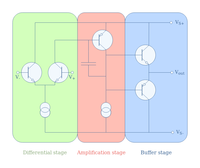
The goal of the differential stage is to pre-amplify the differential signal V+-V– . The special configuration used to realize this process is called a transistor long-tailed pair circuit or differential pair. Moreover, this configuration provides a high input impedance.
The amplification stage is usually a high gain class A amplifier, the capacitor is used to assures the frequency compensation. Note that many amplification stages can be interconnected in order to provide a higher amplification output.
Finally, the buffer stage provides no amplification (unitary gain) but has a low output impedance and, therefore, provides high output currents. It is also used in order to adapt the impedances and protect against short-circuits.
Open-loop gain
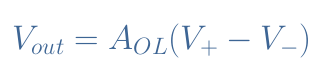
A few major characteristics can be associated with op-amps and we will dictate their electronic behavior here. The first one is the open-loop gain (AOL), it is a factor that represents the amplification applied to the input differential voltage:
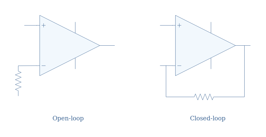
The term “open-loop” refers to the fact that no feedback is applied from the output to the inverting input of the op-amp. We will come back to that notion later on in the tutorial, however, in order to get an idea now of this concept, we show in Figure 3 the distinction made between open-loop and closed-loop op-amps:
Input and output impedances
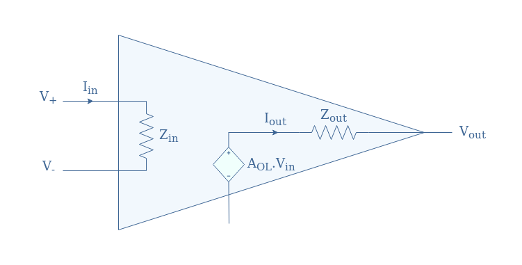
The input impedance Zin represents the ratio Vin/Iin with Vin=V+-V– and Iin being the input current. Similarly, we can also define an output impedance Zout which represents the ratio Vout/Iout with Vout=AOL.Vin and Iout being the output current.
Figure 4 below shows a representation of an op-amp that takes into account these impedances:
Bandwidth
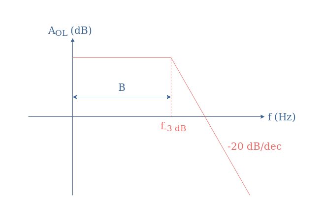
Op-amps can be used in DC but also in the AC regime, such as for example for the amplification of audio signals. For this reason, one of the important characteristics of op-amps is their bandwidth (B). This means that the gain (AOL) is dependent on the input frequency.
The bandwidth is measured in Hertz (Hz) and represents the range of frequencies that an op-amp can amplify efficiently. More precisely, the frequencies for which the gain is higher than -3 dB are included in the bandwidth. The limit frequencies for which the gain is exactly equal to -3 dB are called cutoff frequencies and often labeled f-3dB.
Op-amps behave actually as first-order low-pass filters, this means that the gain can be approximated as a constant from the DC regime up until its cutoff frequency. For higher frequencies, a loss of -20 dB/decade is observed as shown in Figure 5:
To get more detail about this topic, we recommend reading the tutorial about Bode diagrams.
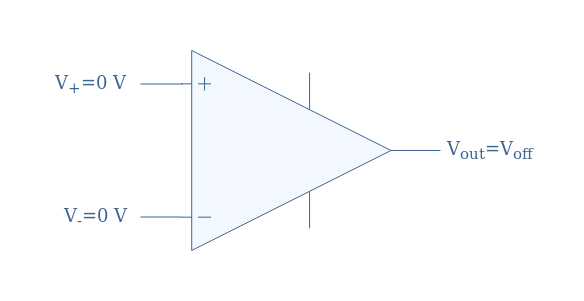
Offset voltage
The offset voltage Voff can be read at the output terminal when no input is applied to the amplifier. For example, if an op-amp has an offset voltage of 1 V, it means that the output voltage will constantly be shifted of +1 V, even when no input signal is applied.
Ideal op-amp model
This model describes an idealized op-amp that is free of any parasitic phenomena. It is of course not possible to build such an op-amp with ideal characteristics but only approach it.
The ideal op-amp model consists of idealizing its main characteristics previously presented in the presentation section:
- Infinite open-loop gain (AOL=+∞)
- Infinite input impedance (Zin=+∞)
- Zero output impedance (Zout=0)
- Infinite bandwidth (B=+∞)
- Zero offset voltage (Voff=0)
This set of idealized characteristics highlights the fact that an ideal op-amp does not disturb the amplified signal. An ideal op-amp is usually represented with a sign “∞” within the triangle shape.
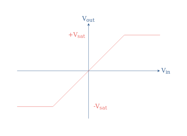
One very important property is that in an open-loop configuration, the output of an ideal op-amp can only take two values called the saturation voltages (Vsat). If the differential input Vin is positive (reciprocally negative), the output is +Vsat (reciprocally -Vsat).
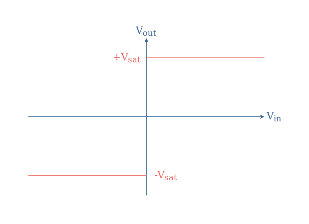
The value of |Vsat| is slightly lower than the absolute value of the supply VS.
In the following subsections, we will see two different modes that can be adopted for an ideal op-amp depending on which input the feedback is applied.
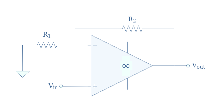
Saturated mode
In this mode, feedback is applied to the non-inverting input (+) of the op-amp. This means that any increase in the output voltage will increase the differential input. This kind of configuration is also known as a comparator and represented in Figure 8:
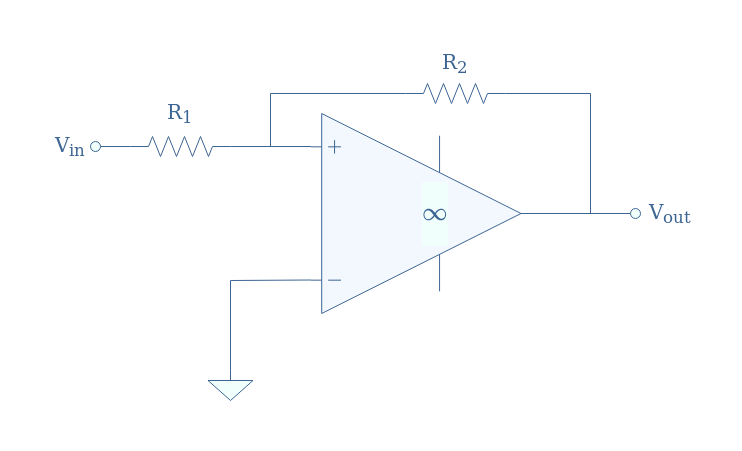
Linear mode
If instead the feedback is applied to the inverting input (-) of the op-amp, the function of the amplifier is completely different.
In this configuration, any increase of the output voltage tends to decrease the differential input and therefore, also tends to maintain a differential input close to zero.
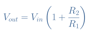
The relation between the input and output voltages is given by Equation 2:
In a closed-loop configuration with negative feedback, the characteristic Vout=f(Vin) is therefore linear according to Equation 2 up until -Vsat and +Vsat where a plateau emerges.
Real op-amps
Op-amps that can be found in real electronic circuits have limited and non-ideal characteristics:
- Finite open-loop gain typically ranges from 105 to 106
- Finite input impedance: 105 up to 1012 Ω
- Non-zero output impedance: 50 to 200 Ω
- Finite bandwidth
- Non-zero offset voltage: 1μV up to 50 mV
The gain of real op-amps depends moreover on the frequency with a variation that can be described as a first order low-pass frequency. Another important information is that the product gain-bandwidth of op-amps is constant, this implies that “slow” op-amps can have higher gains and “fast” op-amps tend to have a lower gain.
The input impedance is not purely resistive as a parallel capacitor of a few pF modelizes the low-pass filter behavior of the op-amp and tends to reduce the impedance when the frequency increases.
Conclusion
We have presented the basics of operational amplifiers in this introductory tutorial. Op-amps are integrated circuits that are powered with two supply inputs and which goal is to amplify the differential input voltage.
We have briefly presented their internal circuitry and shown that at least three stages are necessary to perform amplification.
Many characteristics can define an op-amp, however, five in particular are extremely important and are presented in detail in the first section. Moreover, we explain that two configurations can be adopted leading to different behaviors: the open-loop or closed-loop.
The ideal op-amp model is detailed in a second section where its idealized characteristics and behavior are summarized.
Finally, we highlight the differences between this ideal model and real op-amps that can be found in many modern circuitry. The most important consequences of these differences are the finite gain and bandwidth which limits the amplification and frequency abilities.


