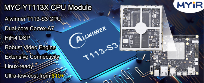
MYIR Launched $14 ARM SoM based on Allwinner T113-S3 dual-core Cortex-A7 SoC
MYIR has launched a new SoM MYC-YT113X based on Allwinner SoC after introduced the MYC-YT507H for T507-H last year. The MYC-YT113X CPU Module is powered by Allwinner T113-S3 processor which features up to 1.2 GHz Dual-core ARM Cortex-A7 processor with 128MB DDR3 on-chip memory.
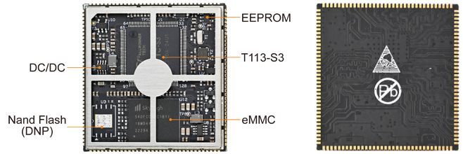
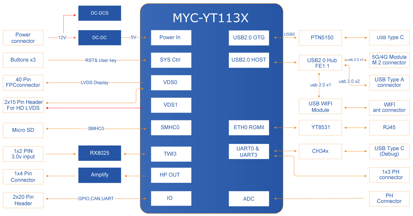
MYIR has launched a new SoM MYC-YT113X based on Allwinner SoC after introduced the MYC-YT507H for T507-H last year. The MYC-YT113X CPU Module is powered by Allwinner T113-S3 processor which features up to 1.2 GHz Dual-core ARM Cortex-A7 processor with 128MB DDR3 on-chip memory. Additionally, the MYC-YT113X takes more other advantages of the T113-S3 MPU such as the single-core HiFi4 DSP, Robust Video Engine and extensive connectivity to provide an ideal solution for smart control and HMI applications in the automotive and industrial sectors. MYIR offers two standard configurations for 256MB Nand Flash or 4GB eMMC external memory options. A number of peripheral and IO signals are access through 1.0mm pitch 140-pin stamp-hole (Castellated-Hole) expansion interface.
The MYC-YT113X CPU Module is a highly integrated SoM, measuring only 39mm by 37mm. It is capable of running Linux and provided with software resources including kernel and driver source code, together with detailed user manual and documentations to help customer start their development rapidly.
Features Of MYC-YT113X CPU Module
- Dimensions: 39mm x 37mm
- PCB Layers: 6-layer design
- Power supply: 5V/1A
- Working temperature: -40~85 Celsius (industrial grade)
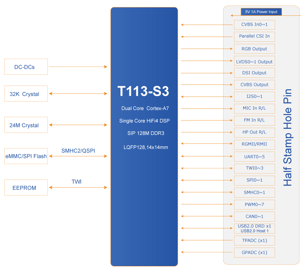
- Allwinner T113-S3 processor
– Up to 1.2GHz Dual-core Arm Cortex-A7 with built-in 128MB DDR3
– Single-core HiFi4 DSP
– Supports H.265/H.264 video decoding up to 1080p@60fps and JPEG/MJPEG video encoding up to 1080p@60fps - 4GB eMMC or 256MB Nand FLASH
- 32KB EEPROM
- 0mm pitch 140-pin stamp hole expansion interface
– 1 x RGMII/RMII
– 2 x USB2.0
– 6 x UART
– 2 x CAN
– 4 x TWI
– 2 x SPI
– 1 x GPADC and 4 x TRADC
– 1 x MIPI DSI
– 1 x Single-channel LVDS and 1 x Dual-channel LVDS or 24-bit RGB (supports up to 1080p@60fps)
– 1 x RGB
– 1 x Parallel CSI
– 2 x I2S
– Up to 59 GPIOs (Note: the peripheral signals brought out to the expansion interface are listed in maximum number. Some signals are reused. Please refer to the processor datasheet and CPU Module pin-out description file) - Linux OS
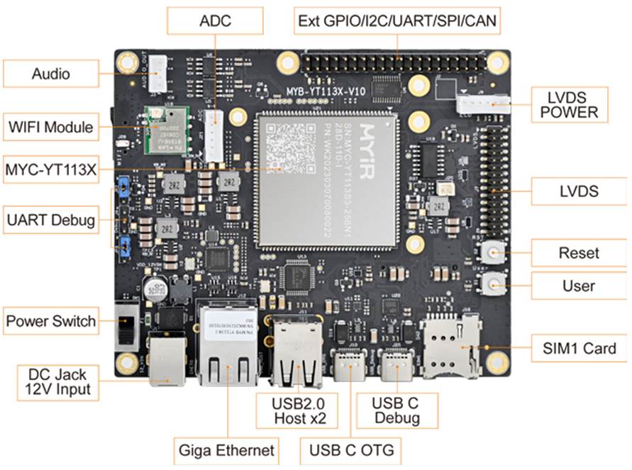
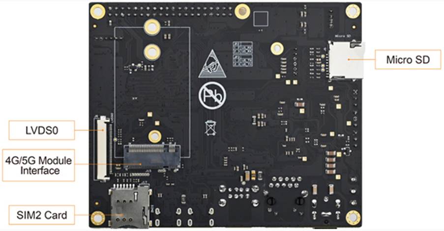
MYIR provides MYD-YT113X Development Board for evaluating the MYC-YT113X CPU Module. It has a versatile base board to facilitate the expansion from the MYC-YT113X through the 140-pin interface, such as serial ports, USB, Ethernet, CAN, WiFi, LVDS, Audio and so on. It is an excellent evaluation platform as well as a solid reference design for customers using the MYC-YT113X CPU Module or solutions based on T113-S3 processors.
The MYC-YT113X CPU Module is a high-performance and ultra-low-cost SoM, pricing at only $14/pc for the 256MB Nand Flash version (MYC-YT113S3-256N128D-110-I). Discount is to be offered for volume quantities. MYIR also provides OEM/ODM services to help customers accelerate their time to market and save cost.
More information about above new products can be found at: https://www.myirtech.com/list.asp?id=722


