Printed circuit board manufacturer – JLCPCB Review
Recently, I had the opportunity to test the printed circuit boards (PCB) offered by JLCPCB. These tests were made in two different boards of the brand and here I’ll report my impressions about them.
Recently, I had the opportunity to test the printed circuit boards (PCB) offered by JLCPCB. These tests were made in two different boards of the brand and here I’ll report my impressions about them.
Due to the spread of the maker culture and the do-it-yourself (DIY) and easy access to components and a huge amount of technical information available on Internet, it has become much simpler to develop a solution to a problem or just have fun soldering some components.
However, taking the design out of a breadboard (or universal board) and turning it into a PCB stills a big challenge, mainly due to the costs involved.
And exactly at this point the services offered by JLCPCB make the difference, offering a high level service of PCB manufacturing with an extremely competitive cost.
Requesting the production of PCBs is quite simple and there are two basic ways to do it. If you are developing within EasyEDA just click on “Gerber Output” and your gerber file will be generated and transferred directly to the JLCPCB system.
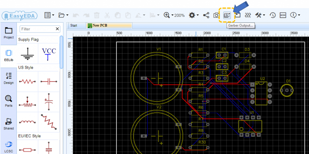
The system will automatically capture PCB informations like dimensions and number of layers.
The second way is useful if you already have the gerber files generated by some tool. Access JLCPCB.com, then click in “Quote now”.
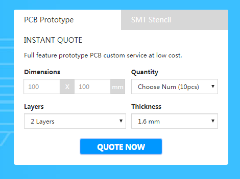
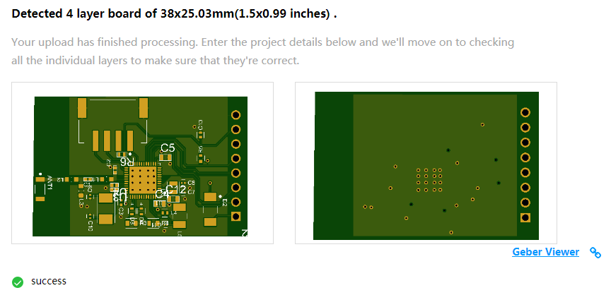
In the next screen, add your gerber files. They need to be compressed in a single .rar or .zip. You can select the compressed file by clicking on “Add your gerber file” or just drag and dropping the file over the button. After the upload the a preview image will be showed and the basic characteristics of pcb will be preconfigured. By clicking in “Gerber view” is possible to visually inspect the gerber of pcb.
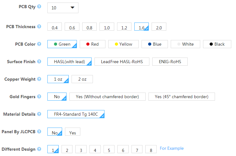
Also in this screen is possible to change PCB definitions like the quantity of ordered pcbs, pcb thickness, pcb color and others.
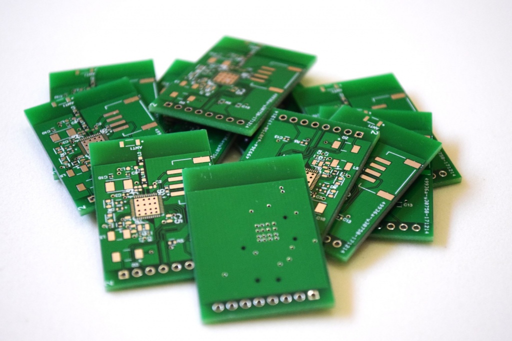
How in my case, I already had the gerber files done, so I just uploaded them to the system. I chose two different projects for this test. The first is a two layers pcb of 79.6mm x 50.8mm, costing just $2.00 for a quantity of 10 pcbs. The second is a four layer pcb of 39mm x 25.5mm, costing $16.42 for a quantity of 10 pcbs. It’s an amazing price for a two layer pcb, and even the four layer has an affordable price, enabling to easily prototype more complex projects.
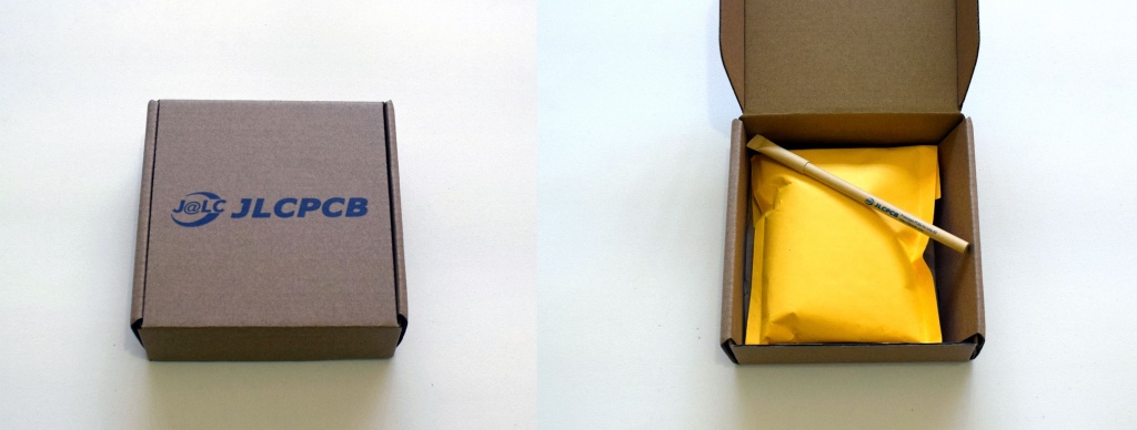
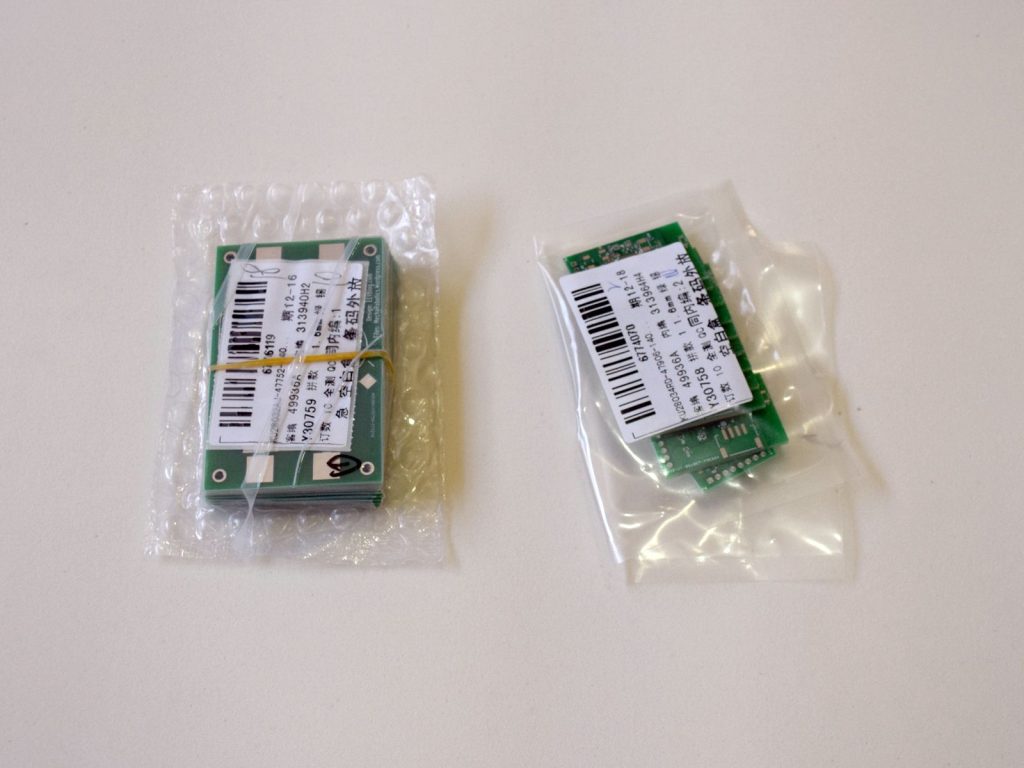
The time between production of pcbs and delivering was 11 calendar days, really fast. The boards had delivered in a JLCPCB logo box. Inside the box, there’re an yellow envelope and a gift pen. The envelope contains the boards nicely packaged with protective plastic, ensuring the integrity of PCBs during the transport.
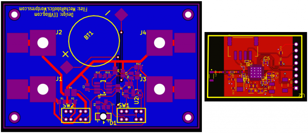
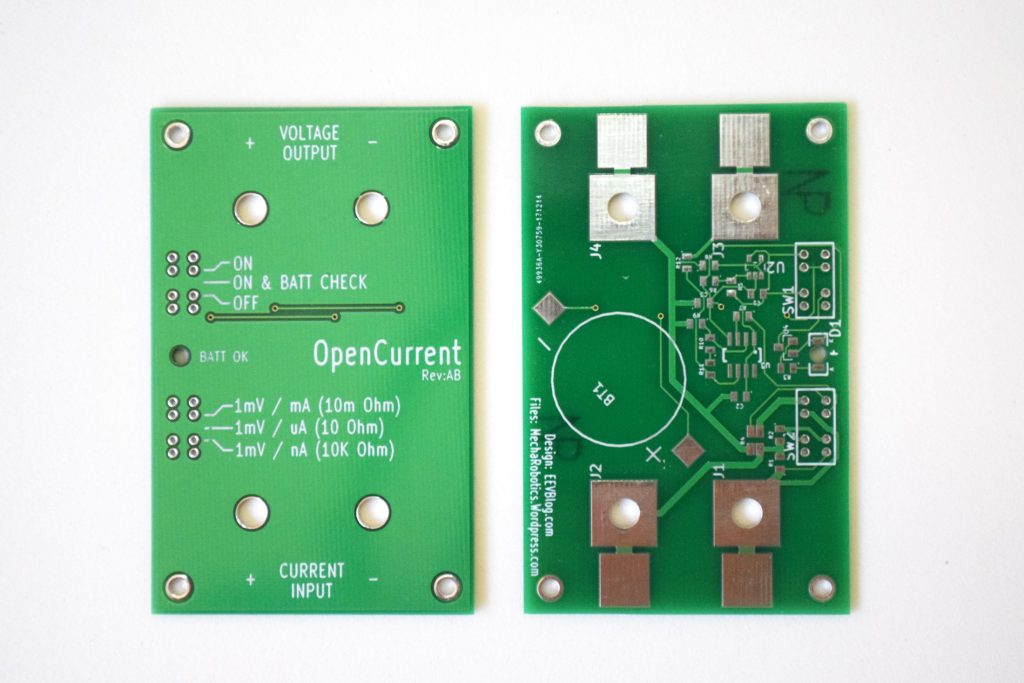
The first board is related to OpenCurrent, an open source version of uCurrent developed by Dave Jones of the EEVblog. The board has two layers and their dimensions are approximately 80mm x 51mm. The top layer is basically a ground plane with only two tracks in addition to the silks indicating the features of the connectors and switches. In the bottom layer there’s the connectors soldering pad, the components and connection tracks.
The second PCB refers to a small BLE module. It’s a fairly small board with dimensions reaching approximately 39mm x 26mm. Also, it has 4 layers to guarantee the requirements of a project involving RF. The board uses several small SMD components, rather thin tracks as well as vias between the layers.
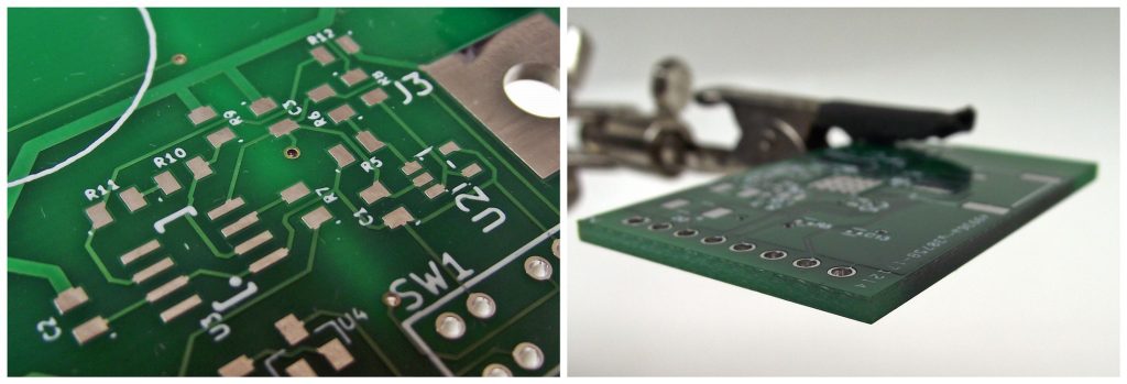
The service quality is, doubtless, a highlight point in both boards. The board manufacturing process guarantees well-defined and faultless traces, from the widest tracks in the OpenCurrent pcb to the finer tracks present in the small BLE module. In addition, the copper layer has a good thickness.
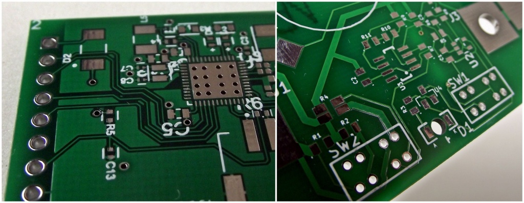
The solder mask is evenly distributed on both sides without fail, giving a beautiful glossy finish to PCB. The alignment of the solder mask is excellent in all boards, no trespassing any solder pad, even in the smallest SMD components or in the pads of BLE SoC. This avoiding unwanted hard-to-find short circuits, helping a lot when we’re soldering components.
Another point that claims a lot of attention is the silk screen quality. Note that the silks are slightly larger than the traces and still remain readable. Finally, the finish cutting and drilling of boards is also excellent. All boards have the same size and their edges don’t have burrs.
I can say that I’m quite impressed with the service quality provided, especially considering its low cost. Therefore, it becomes much simpler to bring a prototype to life. Definitely, It’s worth to use the service offered by JLCPCB.


https://www.youtube.com/watch?v=vQb4U8wAzH8
I also ordered from them and I recorded a video about quality and how to order
Don’t waste your time on this. It’s nothing more than an a PCB vendor promotion. No schematic, no theory of operation, incomplete parts list. It is not possible to replicate the project with the information provided. This is yet another
junk circuit from JLCPCB.